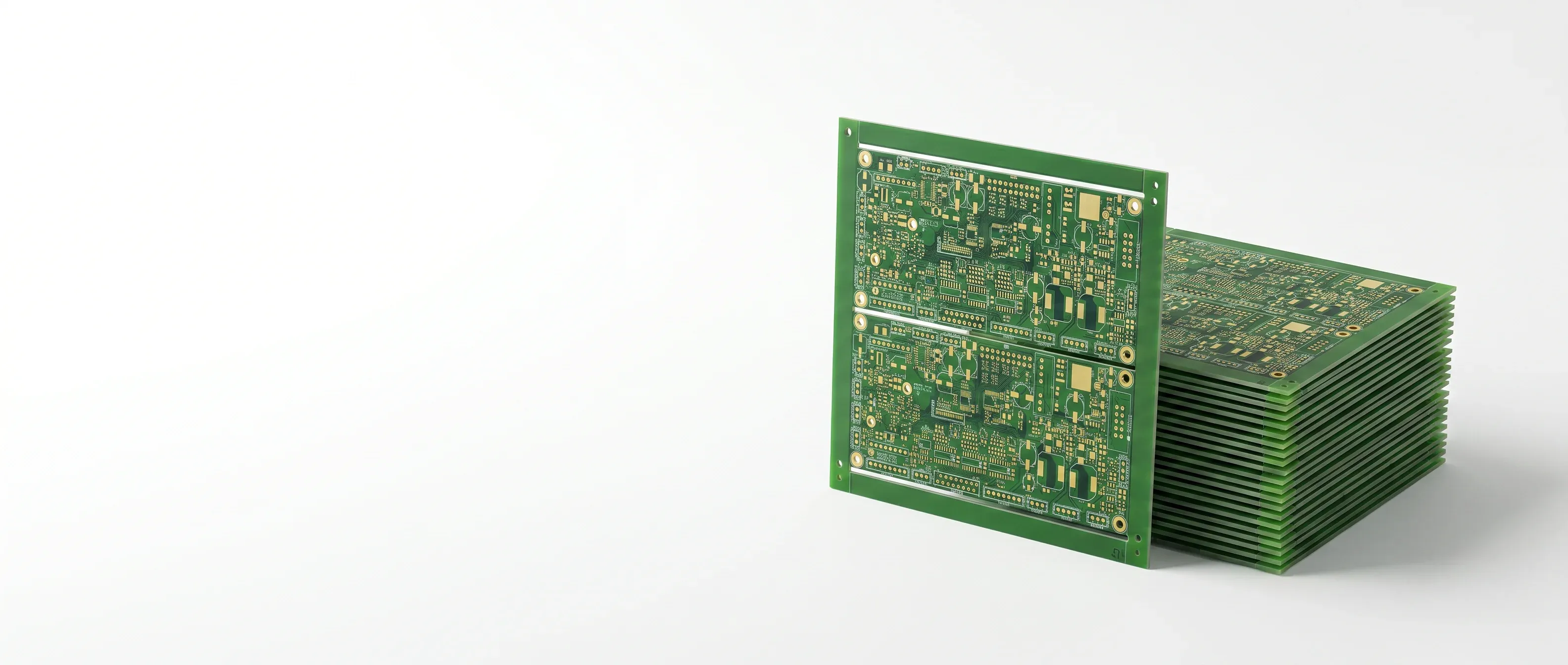
Multilayer PCB Manufacturing
Multilayer PCB Manufacturer 2 to 30 Layers, Precision Built
Up to 30 layers. 3/3mil trace. ±8% impedance. Every board engineered for first-pass success.
Layer Count Guide
Multilayer PCB Fabrication (4 / 6 / 8 / 10+ Layers)
Our multilayer PCB fabrication spans 2 to 30 impedance-controlled layers, so a single multilayer printed circuit board can carry dense digital routing, controlled-impedance pairs, and solid power planes in one symmetrical stack. For an industrial control PCB — motor drives, PLC backplanes, sensor fusion — those added ground and power planes are what keep switching noise off the sensitive analog and signal nets.
4-Layer
The entry point for a controlled-impedance multilayer PCB: signal / ground / power / signal. Choose 4 layers when a 2-layer board can no longer give you a continuous reference plane under high-speed traces.
6-Layer
Two routing layers plus dedicated plane pairs. The workhorse stackup for dense digital designs and most 0.8mm-pitch BGA breakouts that still route cleanly without HDI.
8-Layer
Additional plane pairs tighten return paths and impedance targets for high-speed interfaces, DDR, and boards mixing sensitive analog with fast digital sections.
10+ Layers
Up to 30 layers with sequential lamination, precise registration, and symmetrical stackups for warpage control — for backplanes, telecom line cards, and complex industrial control PCBs.
Capabilities
When Your Design Pushes Boundaries
Built for signal integrity from the first plane pair up. Our factory selection ensures your 20+ layer board goes to a facility with proven capability at that layer count — not one that will "try their best."
High Layer Count
Up to 30 layers with sequential lamination and precise registration. Symmetrical stackups optimized for warpage control.
Controlled Impedance
Single-ended 50Ω, differential 100Ω, or custom targets. ±8% tolerance with coupon verification.
Heavy Copper
Up to 6oz outer / 3oz inner for power electronics. Thick copper plating on the same board as fine signal traces.
Blind & Buried Vias
Reduce via stubs, increase routing density. Via-in-pad with copper fill for BGA designs.

Multilayer Boards We Build
Layer counts from 4 to 30 — in the wild


Stackup Engineering
How We Build Your Stackup
We treat stackup design as an engineering exercise, not a template lookup. These are the decisions we make on every multilayer board before a single sheet of prepreg is cut.
Symmetry & Copper Balance
A 12-layer board is arranged so layers 1-6 mirror 7-12 in copper weight, dielectric, and prepreg — asymmetrical stacks bow and twist as resin cures. We check copper distribution on every layer pair; if layer 3 is 80% fill but layer 10 is 20%, we add copper thieving or reorder the stackup to rebalance before production.
Reference Plane Pairing
Every high-speed signal layer sits against a continuous ground or power plane. A typical 8-layer arrangement — Signal / Gnd / Signal / Pwr / Pwr / Signal / Gnd / Signal — gives the inner signal layers uninterrupted references above and below for stripline impedance and crosstalk shielding. We never place two signal layers adjacent above 1 Gbps.
Dielectric Thickness Control
We hold prepreg thickness to ±0.5mil, so a 4.0mil target lands between 3.5-4.5mil — roughly ±4% impedance on a 50Ω trace. Thinner glass styles compress more uniformly, so for critical layers we often specify two sheets of 1080 (2.8mil cured) over one sheet of 2116 for tighter uniformity, even at the same total thickness.
Material Selection
Standard FR-4 TG150 for single lead-free reflow (260°C peak); TG170 for double-sided assembly and rework (4-5 reflow passes); Isola 370HR (TG180, Td 340°C) for aerospace/automotive CAF resistance. For >10 Gbps, Panasonic Megtron 6 (Df 0.004 at 10GHz) cuts insertion loss ~40% versus standard FR-4 (Df 0.020).
Copper Weight
Inner layers run 0.5oz (17μm) for fine-pitch signal or 1oz (35μm) default; 2oz (70μm) for high-current planes, where trace minimums rise from 3mil to 5mil due to etch undercut. Outer layers start at 1oz base, plated to 1.5-2oz. Heavy copper (3-6oz) gets modified etch parameters and wider annular rings, confirmed by DFM early.
Lamination Press Cycle
The book laminates on a precise profile: ramp to 130°C at 2-3°C/min, hold 15 min for uniform flow, ramp to 180°C at 2°C/min, hold 60 min for full cure, then cool at 3°C/min. Pressure runs 50 PSI during flow to 300 PSI during cure; vacuum below 10 mbar throughout kills entrapped air. Roughly 3-4 hours per press load.
Impedance Control & Verification
We manage trace width, dielectric height, and copper weight together — a 50Ω microstrip at 4mil height needs ~7mil trace at 1oz, ~6mil at 3.5mil height. Every controlled-impedance stackup is modeled in Polar Si9000, then verified by TDR on production coupons that ride the same panel through identical processing.
Blind & Buried Vias
Buried vias (e.g. L3-L4) are drilled and plated as a sub-lamination before the main press; blind vias (L1-L2) are controlled-depth drilled after final lamination. Both free routing space and remove high-speed stubs. We hold a 4mil minimum annular ring and verify layer-to-layer registration with X-ray before drilling.

Materials & Stackup
Matched to your reflow and Df budget
We select the laminate to your thermal and signal budget rather than defaulting to one grade. Standard FR-4 TG150 covers single lead-free reflow (260°C peak); TG170 is our default for double-sided assembly and rework that sees 4-5 reflow passes; and Isola 370HR (TG180, Td 340°C) adds CAF resistance for aerospace and automotive builds.
For high-speed layers above 10 Gbps, Panasonic Megtron 6 (Df 0.004 at 10GHz) cuts insertion loss roughly 40% versus standard FR-4 (Df 0.020). Dielectric height is built from 1080 (2.8mil), 2116 (4.6mil), and 7628 (7.0mil) prepreg over cores from 2mil to 62mil, combined to hit custom stackup targets within ±10%.
Applications
Where our multilayer boards go
When boards can't fail, engineering oversight makes the difference — trusted in critical applications across networking, compute, industrial, and automotive.

Networking & Telecom
High-speed switch fabrics, 400G optical modules, base station power amplifiers.

Data Center & Compute
High-layer-count backplanes and line cards for switch fabrics, servers, and AI compute infrastructure.

Industrial Controls
Motor drives, PLC backplanes, sensor fusion boards for harsh environments.

Automotive Electronics
ADAS processing, battery management, infotainment — automotive-grade production.
What Sets Us Apart
Not Your Average Board House
We specialize in the boards that other shops struggle with.
3/3mil Fine-Pitch Routing
Break out 0.5mm BGA without HDI. Our advanced imaging and etching lines maintain consistent trace geometry at 75μm features.
±8% Impedance Control
Dielectric thickness precision with TDR verification on every controlled-impedance order. Reports ship with your boards — not on request.
Engineering Before Production
A human engineer reviews your stackup, material selection, and DFM before any panel touches a production line. Issues caught here, not at assembly.
5-Day Prototype Turnaround
Standard 5-day lead time for 1-2 layer boards. Rush options available, reducing lead time by up to 4 days (minimum 1-day turnaround).
High-TG for Lead-Free
TG170 material standard for complex multilayer builds. Survives multiple reflow cycles without delamination.
Full Documentation
Impedance reports, material certificates, electrical test results, cross-section photos for critical builds. Standard, not add-ons.
FAQ
Common Questions
30 layers for standard FR-4 builds. For designs requiring more density, our HDI process achieves equivalent routing in fewer layers through sequential lamination and microvias.
±8% with TDR test coupon verification on every impedance-controlled order. Reports ship with your boards automatically.
HASL, lead-free HASL, ENIG (up to 50U"), hard gold, OSP, immersion silver, immersion tin, and ENEPIG for wire bonding applications.
5 days standard for 1-2 layer boards. Rush options reduce lead time by up to 4 days (minimum 1-day turnaround). Complex multilayer (16+ layers) starts at 12 days standard.
Cores from 2mil to 62mil thickness. Standard prepreg glass styles: 1080 (2.8mil cured), 2116 (4.6mil cured), 7628 (7.0mil cured). We combine multiple prepreg sheets for custom dielectric heights — for example, two sheets of 1080 gives 5.6mil, which is different from one sheet of 2116 at 4.6mil. Laminated thickness tolerance is ±10% of the target dielectric height.
Yes. The most common hybrid is FR-4 core with Megtron 6 prepreg on signal layers — you get improved Df (0.004 vs 0.020) on the critical high-speed layers without paying for full high-speed laminate on power and ground planes. We also build Rogers/FR-4 hybrid stackups for boards that combine RF front-end with digital baseband on the same PCB.
Four controls: symmetrical stackup design (mirrored layer arrangement), copper balancing on every layer pair (thieving patterns where needed), controlled lamination ramp rates (2-3°C/min prevents thermal shock), and post-cure stress relief (4-hour bake at 150°C for panels above 16 layers). For boards exceeding 16 layers, we run warpage simulation before production and reject stackup proposals that predict bow/twist above IPC-6012 limits (0.75% for SMT boards).
Ready to Build?
Upload your Gerbers. Get an instant quote with engineering review included.
Resources
Multilayer PCB Engineering Guides
Stackup design, impedance control, and DFM optimization for multilayer rigid boards.
16-Layer PCB Stackup Design: Rules, Impedance Planning & Material Selection
Practical stackup design rules for high-layer-count FR-4 boards.
How to Specify Controlled Impedance on Your Fab Drawing
Step-by-step DFM guide for impedance table format and tolerance callouts.
PCB Design Rules for Minimum Fabrication Cost
DFM guidelines that directly reduce PCB fabrication price.
PCB Rush Pricing Explained: Lead Time vs Cost Tradeoffs
How lead time affects fabrication cost and strategies to minimize rush fees.
Tg150 vs Tg170 FR-4: Choosing the Right Glass Transition Temperature
Engineering decision guide with CTE data and application recommendations.
How to Specify Backdrilling in PCB Fab Notes
Depth tolerances, drawing callouts, and common mistakes for via stub removal.