· AtlasPCB Engineering · Engineering · 7 min read
16-Layer PCB Stackup Design: Rules, Impedance Planning & Material Selection
Complete engineering guide to 16-layer PCB stackup design. Covers layer assignment strategies, impedance planning, material selection for high-speed signals, power distribution, and manufacturing constraints for complex multilayer boards.
16-Layer PCB Stackup Design: Rules, Impedance Planning & Material Selection
Designing a 16-layer PCB stackup is where signal integrity theory meets manufacturing reality. With 16 layers, you have enough routing resources for complex designs—high-pin-count FPGAs, multi-channel high-speed SerDes, and dense power distribution networks—but the stackup decisions you make directly determine whether those signals propagate cleanly or suffer from crosstalk, impedance discontinuities, and EMI failures.
This guide walks through the complete 16-layer stackup design process: layer assignment strategy, impedance planning, material selection, power distribution, and the manufacturing constraints that your fabricator needs you to understand before you send Gerbers.
Why 16 Layers? The Design Complexity Threshold
A 16-layer board is typically required when your design has:
- High-pin-count BGAs (1000+ pins) requiring 4+ breakout routing layers
- High-speed serial interfaces (PCIe Gen 4/5, 25G+ Ethernet, USB4) needing dedicated impedance-controlled layers with adjacent ground references
- Complex power distribution requiring 2+ dedicated power planes for multiple voltage rails
- Dense analog/digital mixed-signal designs needing physical separation between domains
- Thermal management requirements using internal copper planes for heat spreading
The 16-Layer Advantage Over 12 Layers
Moving from 12 to 16 layers provides critical benefits:
| Benefit | 12-Layer | 16-Layer |
|---|---|---|
| Signal layers | 6 | 8 |
| Reference planes | 6 | 8 |
| Signal-to-reference ratio | 1:1 (ideal) | 1:1 (ideal) |
| BGA breakout layers | 3–4 | 4–6 |
| Power plane count | 2 | 2–3 |
| Dedicated ground planes | 4 | 4–5 |
| Routing density | Moderate | High |
The additional 4 layers eliminate the routing congestion that forces compromises in 12-layer designs—like routing high-speed signals on layers without adjacent ground planes or sharing power planes between incompatible voltage domains.
Recommended 16-Layer Stackup Configurations
Configuration A: Balanced High-Speed (Recommended)
This is the go-to stackup for most high-speed digital designs:
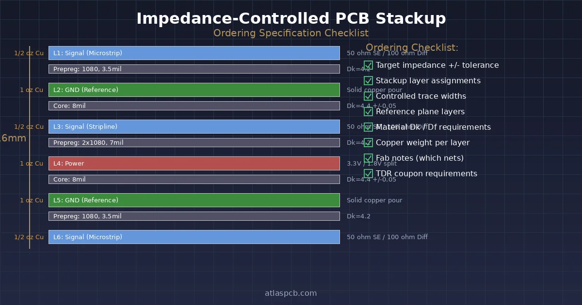
| Layer | Function | Copper Weight | Target Impedance |
|---|---|---|---|
| L1 | Signal (Top) | 1 oz | 50Ω SE / 100Ω diff |
| L2 | Ground | 1 oz | Reference |
| L3 | Signal | 0.5 oz | 50Ω SE / 100Ω diff |
| L4 | Power (3.3V/1.8V) | 1 oz | Distribution |
| L5 | Signal | 0.5 oz | 50Ω SE / 100Ω diff |
| L6 | Ground | 1 oz | Reference |
| L7 | Signal | 0.5 oz | 50Ω SE / 100Ω diff |
| L8 | Ground | 1 oz | Reference |
| L9 | Ground | 1 oz | Reference |
| L10 | Signal | 0.5 oz | 50Ω SE / 100Ω diff |
| L11 | Ground | 1 oz | Reference |
| L12 | Signal | 0.5 oz | 50Ω SE / 100Ω diff |
| L13 | Power (1.0V/1.2V) | 1 oz | Distribution |
| L14 | Signal | 0.5 oz | 50Ω SE / 100Ω diff |
| L15 | Ground | 1 oz | Reference |
| L16 | Signal (Bottom) | 1 oz | 50Ω SE / 100Ω diff |
Key features:
- Every signal layer has an adjacent ground or power plane
- L8/L9 ground-ground pair creates a natural symmetry axis
- Two power planes (L4, L13) positioned symmetrically
- 8 signal layers provide ample routing resources
Configuration B: Maximum Routing Density
For BGA-intensive designs requiring maximum escape routing:
| Layer | Function | Notes |
|---|---|---|
| L1 | Signal (Top) | Component placement, short traces |
| L2 | Ground | Primary reference |
| L3 | Signal | BGA breakout layer 1 |
| L4 | Signal | BGA breakout layer 2 |
| L5 | Ground | Reference for L3/L4 |
| L6 | Signal | High-speed routing |
| L7 | Power (Core) | Primary power |
| L8 | Ground | Core reference |
| L9 | Ground | Core reference |
| L10 | Power (Core) | Secondary power |
| L11 | Signal | High-speed routing |
| L12 | Ground | Reference for L13/L14 |
| L13 | Signal | BGA breakout layer 3 |
| L14 | Signal | BGA breakout layer 4 |
| L15 | Ground | Primary reference |
| L16 | Signal (Bottom) | Component placement |
Warning: Configuration B places signal layers L3/L4 and L13/L14 adjacent to each other without an intervening ground plane. This creates crosstalk risk and is only acceptable for low-speed signals (< 100 MHz). High-speed differential pairs must be routed on layers with adjacent ground reference (L6, L11).
Impedance Planning for 16-Layer Boards
Dielectric Thickness Requirements
For 50Ω single-ended impedance with 1 oz copper:
| Trace Width | Dielectric to Reference | Configuration |
|---|---|---|
| 4.0 mil | 3.0–3.5 mil | Microstrip (outer) |
| 4.5 mil | 4.0–4.5 mil | Microstrip (outer) |
| 3.5 mil | 3.5–4.0 mil | Stripline (inner) |
| 4.0 mil | 4.5–5.0 mil | Stripline (inner) |
For 100Ω differential pairs:
| Trace Width | Spacing | Dielectric | Configuration |
|---|---|---|---|
| 4.0 mil | 4.0 mil | 3.0–3.5 mil | Edge-coupled microstrip |
| 3.5 mil | 5.0 mil | 4.0 mil | Edge-coupled stripline |
| 4.0 mil | 6.0 mil | 4.5 mil | Broadside-coupled stripline |
These values assume FR4 with Dk ≈ 4.2 at 1 GHz. For high-Tg materials (Dk ≈ 4.0), trace widths increase approximately 5%. Always request impedance modeling from your fabricator using their actual prepreg and core Dk values—published datasheets can deviate ±5% from production lots.
Stackup Thickness Budget
A typical 2.4mm (94 mil) 16-layer stackup budget:
| Element | Thickness | Quantity | Subtotal |
|---|---|---|---|
| Outer copper (1 oz) | 1.4 mil | 2 | 2.8 mil |
| Inner copper (0.5 oz) | 0.7 mil | 14 | 9.8 mil |
| Prepreg layers | 3.5 mil avg | 15 | 52.5 mil |
| Core layers | 2–4 mil | Variable | 28.9 mil |
| Total | 94.0 mil |
The prepreg and core thickness allocation must balance impedance targets against total board thickness. Thinner dielectrics enable tighter impedance control but increase manufacturing sensitivity.

Material Selection for 16-Layer Boards
Standard vs Low-Loss Materials
| Data Rate | Recommended Material | Dk @ 1GHz | Df @ 1GHz | Cost Factor |
|---|---|---|---|---|
| < 5 Gbps | High-Tg FR4 (370HR) | 4.04 | 0.021 | 1.0× |
| 5–10 Gbps | Mid-loss (Megtron 4) | 3.83 | 0.005 | 1.8× |
| 10–25 Gbps | Low-loss (Megtron 6) | 3.71 | 0.002 | 3.0× |
| > 25 Gbps | Ultra-low-loss (Tachyon) | 3.02 | 0.0015 | 4.5× |
For most 16-layer designs running PCIe Gen 3/4 or 10G Ethernet, high-Tg FR4 (Isola 370HR or equivalent) provides adequate performance. The transition to low-loss materials becomes necessary when channel loss exceeds the receiver’s equalization capability—typically above 10 Gbps for traces longer than 6 inches.
Hybrid Stackup Strategy
For cost-sensitive designs with a few high-speed channels:
- Critical signal layers (e.g., L3, L14 carrying SerDes): Low-loss core material
- All other layers: Standard high-Tg FR4
- Result: 40–60% cost savings vs. full low-loss stackup
This hybrid approach requires careful material compatibility validation—CTE mismatch between different laminate systems can cause reliability issues during thermal cycling. Consult the [PCB material selection guide]/blog/pcb-material-selection-guide/) for compatibility matrices.
Power Distribution Design
Plane Pair Impedance
For effective high-frequency decoupling, the impedance of the power-ground plane pair should be minimized. Plane pair impedance is:
Z_planes = (377 / √εr) × (h / w)
Where h is the dielectric thickness between planes and w is the plane extent. For 16-layer boards:
- Place power and ground planes on adjacent layers (e.g., L4-L5 or L7-L8)
- Use thin dielectric (2–3 mil) between power-ground pairs for maximum capacitance
- Each power-ground plane pair provides approximately 30–50 pF/cm² of distributed capacitance
Multiple Voltage Domain Management
A 16-layer design typically needs 3–6 voltage rails. Strategies for efficient power distribution:
- Dedicated power planes: Use L4 for higher-current rails (3.3V, 1.8V) and L13 for lower-current rails (1.0V, 1.2V)
- Split planes: Divide a single power layer into isolated regions for different voltages—but avoid routing high-speed signals across split plane boundaries
- Embedded power routing: For low-current rails (< 500mA), route as wide traces on signal layers rather than consuming plane layers
Manufacturing Considerations
Sequential Lamination
16-layer boards with blind/buried vias require sequential lamination—building the board in stages rather than a single press cycle:
- 2-stage buildup: Inner 8 layers laminated first, then outer layers added
- 3-stage buildup: Required for complex via structures (buried vias + blind vias)
- Cost impact: Each additional lamination stage adds 20–30% to fabrication cost
For through-hole-only designs, a single lamination cycle with precise [registration alignment]/blog/multilayer-pcb-manufacturing-process-explained/) is sufficient.
Via Structure Planning
| Via Type | Layer Span | Drill Method | Aspect Ratio Limit |
|---|---|---|---|
| Through-hole | L1–L16 | Mechanical | 10:1 (0.2mm drill in 2.0mm board) |
| Blind via | L1–L3 or L14–L16 | Laser + mechanical | 1:1 (laser portion) |
| Buried via | L3–L14 (example) | Mechanical | 8:1 |
| Microvia | L1–L2 or L15–L16 | Laser | 0.75:1 |
Plan your via structure early—it determines the lamination sequence, which impacts cost, lead time, and minimum feature capabilities. Refer to the [multilayer PCB stackup design guide]/blog/multilayer-pcb-stackup-design-guide/) for detailed via planning methodology.
Registration and Alignment
With 16 copper layers, registration accuracy compounds through the stackup:
- Layer-to-layer registration: ±2 mil typical, ±1 mil for HDI
- Cumulative registration L1-to-L16: ±4–6 mil for standard process
- Impact on annular ring: Minimum annular ring must account for worst-case misregistration
Design annular rings with ≥ 4 mil on inner layers and ≥ 5 mil on outer layers to accommodate registration tolerance in 16-layer constructions.
Signal Integrity Verification Checklist
Before finalizing your 16-layer stackup:
- Every high-speed signal layer has an adjacent ground reference plane
- No high-speed signals cross split plane boundaries
- Differential pair spacing and trace width verified for target impedance
- Via stub length acceptable (< λ/20 at highest frequency) or back-drilling specified
- Power-ground plane pairs use minimum practical dielectric thickness
- Return current paths identified for every critical signal transition between layers
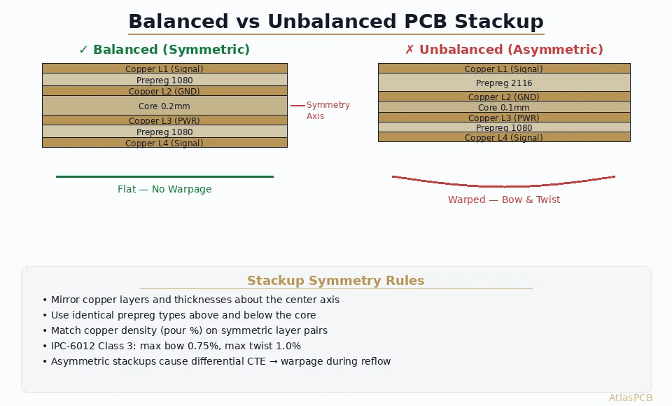
- Stackup is symmetrical about the center axis to prevent warpage
Verified stackup designs with proper [impedance control specifications]/blog/pcb-impedance-control/) are the foundation of reliable 16-layer PCB manufacturing.
Summary
A 16-layer stackup requires careful balance between signal integrity, power distribution, manufacturability, and cost. The recommended Configuration A (alternating signal-ground layers with symmetrical power plane placement) provides the best performance for most high-speed digital designs.
Ready to validate your 16-layer stackup? Upload your design files for a free engineering review including impedance modeling and DFM analysis.
Further Reading
- [Multilayer PCB Stackup Design Guide: 8 to 30+ Layers]/blog/multilayer-pcb-stackup-design-guide/)
- [PCB Impedance Control: How to Achieve ±5% Tolerance]/blog/pcb-impedance-control/)
- [PCB Material Selection Guide: FR4, Rogers, Polyimide & More]/blog/pcb-material-selection-guide/)
- [Signal Integrity in PCB Design: Crosstalk, Reflections & Solutions]/blog/signal-integrity-pcb-design-guide/)
About AtlasPCB — We specialize in complex PCB manufacturing for HDI, RF, and high-reliability applications. Explore our impedance-controlled PCB manufacturing . Every order includes free engineering review. Get your quote.
Reviewed by AtlasPCB Engineering Team — IPC-certified manufacturing specialists with 15+ years of production experience in HDI, RF, and high-reliability PCB fabrication. Content based on factory floor data and real customer design reviews.
- stackup-design
- multilayer-pcb
- impedance-control
- high-speed-design