· AtlasPCB Engineering · Engineering · 10 min read
How to Specify Controlled Impedance on Your PCB Fab Drawing: A Complete DFM Guide
Step-by-step guide for specifying impedance requirements on your fabrication drawing, including table format, tolerance callouts, reference layers, and common mistakes that cause re-spins.
The 30-Second Version
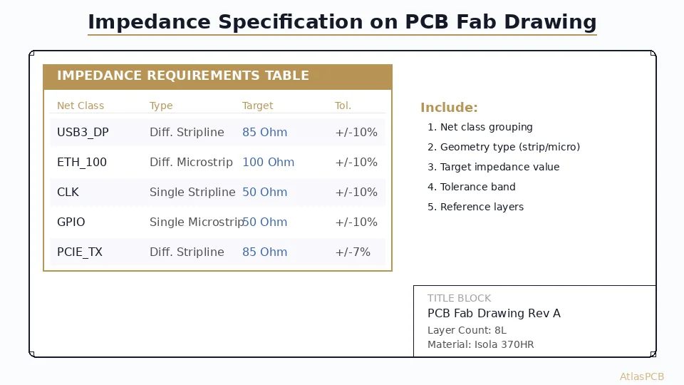
Your fab drawing impedance table needs exactly five columns: Net Class, Geometry Type (microstrip/stripline), Target Impedance (Ohms), Tolerance (+/-%), and Reference Layers. That is it. Do not specify trace width — let the fabricator calculate it from their actual material properties. Include a note stating “Fabricator to adjust trace width to achieve target impedance” and reference IPC-2141A for measurement methodology.
Why Your Fab Drawing Is the Single Source of Truth
Every year, our DFM team catches roughly 200 impedance-related specification errors across customer submissions. The most common failure mode is not a wrong impedance value — it is ambiguity. When your Gerber files show a 5-mil trace but your fab notes say “100 Ohm differential,” and the stackup requires 4.2-mil traces to achieve that impedance on the actual material, we have a conflict that requires an engineering query. That query costs you 24-48 hours of lead time.
The fab drawing is not a formality. It is the legal contract between you and your fabricator. If the impedance table is clear, complete, and internally consistent with your stackup, the board gets built right the first time. If it is vague or contradictory, you get an email asking for clarification — or worse, a board that technically meets your drawing but fails functionally because the fabricator interpreted your intent differently than you meant it.
In our production facility, boards with properly specified impedance tables move through engineering review in under 2 hours. Boards with incomplete or conflicting specs average 3-4 days in the query queue. The difference between a 5-day and an 8-day delivery often comes down to how well the impedance was specified up front.
DFM REVIEW
Upload Your Design for Impedance Verification
Our engineers validate your impedance specs against your stackup before production — catching conflicts early.
Upload Gerber Files ›The Impedance Table: Required Fields and Format
Your impedance specification table should appear prominently on page 1 of your fab drawing (not buried in notes on page 3). Here is the format we recommend based on processing thousands of impedance-controlled designs:
| Net Class | Type | Target (Ohm) | Tolerance | Ref Layers | Notes |
|---|---|---|---|---|---|
| USB3_DP | Diff Stripline | 90 | +/-10% | L3-L4 (GND) | Per USB 3.2 spec |
| ETH_MDIO | Diff Microstrip | 100 | +/-10% | L2 (GND) | — |
| PCIE_TX | Diff Stripline | 85 | +/-7% | L5-L6 (GND) | Gen 5 channel |
| CLK | SE Stripline | 50 | +/-10% | L3-L4 (GND) | Spread-spectrum |
| DDR4_DQ | SE Microstrip | 40 | +/-10% | L2 (GND) | JEDEC JESD79-4 |
Critical formatting rules:
Specify “Differential Stripline” or “Single-ended Microstrip” — never just “50 Ohm” without geometry context. A 50-Ohm microstrip and a 50-Ohm stripline require completely different trace widths, and the fabricator needs to know which you intend. If your schematic tool exports a net class list, map each class to its routing layer and geometry before adding it to the fab drawing.
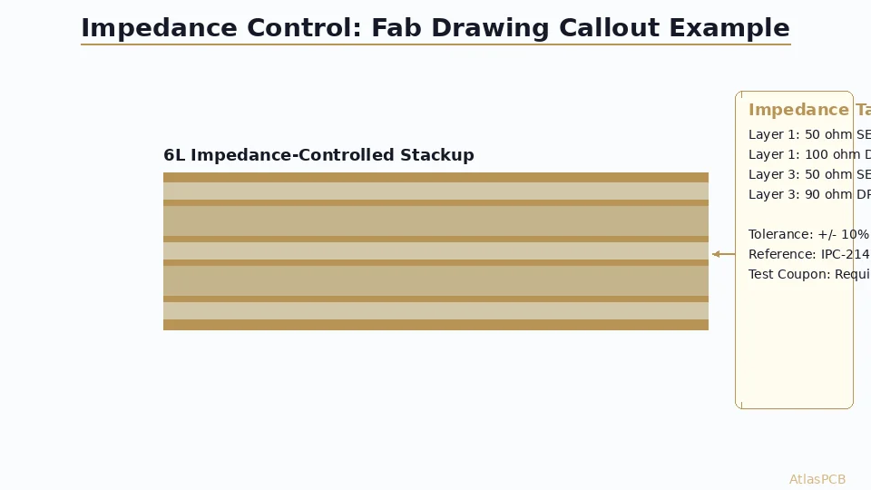
The reference layer column eliminates ambiguity for asymmetric striplines. In a 12-layer board, Layer 7 signals might reference Layer 6 (ground) above and Layer 8 (power) below — with different copper fill percentages on each. Calling out the reference explicitly tells the fabricator which dielectric thickness to use in their impedance calculation.
The Five Most Common Impedance Specification Mistakes
Our DFM engineering team tracks the most frequent impedance errors we see. These five account for 85% of all impedance-related engineering queries:
1. Specifying both trace width AND impedance. This creates a mathematical conflict. Your layout tool calculated 4.8-mil traces based on ideal material properties. The fabricator’s actual material has slightly different Dk (3.9 vs 4.0), requiring 4.5-mil traces. If you lock both parameters, one must lose. Always add the note: “Impedance takes priority over trace width. Fabricator may adjust width +/-0.5 mil to meet impedance target.”
2. Missing impedance spec for differential pairs. We see boards where single-ended nets are spec’d at 50 Ohm but the differential pairs (which are actually more critical) have no impedance callout. If it routes as a pair, it needs a differential impedance target. Common values: USB 90 Ohm, Ethernet 100 Ohm, PCIe 85 Ohm, HDMI 100 Ohm.
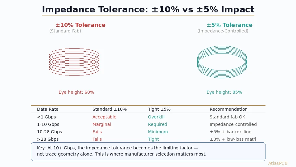
3. Tolerance too tight for the design. Specifying +/-5% on a standard FR-4 board with 62-mil thickness is unrealistic without process premium. The natural variation in FR-4 Dk (3.8-4.2 per IPC-4101) makes +/-5% impractical unless you specify a controlled-Dk material and accept the 15-30% cost increase.
4. No reference to measurement standard. Add “Impedance measured per IPC-TM-650, Method 2.5.5.7 (TDR)” to your notes. This defines the measurement methodology, test coupon geometry, and acceptance criteria. Without it, the fabricator’s QC team may use different measurement conditions that yield different results.
5. Mixing up odd-mode and differential impedance. Differential impedance = 2 x odd-mode impedance (approximately). If your SI tool reports odd-mode impedance of 42.5 Ohm, your differential impedance target should be 85 Ohm, not 42.5 Ohm. We catch this error roughly once per month and it always requires a phone call to clarify.
AVOID COSTLY RESPINS
Pre-Production DFM Review Included
We check impedance specs, stackup consistency, and manufacturability before cutting tooling.
Stackup Coordination: Bridging Design and Fabrication
Your impedance spec does not exist in isolation — it is inseparable from your stackup. The most robust approach is to include a preliminary stackup drawing alongside your impedance table, then add the note: “Final stackup subject to fabricator optimization to meet impedance targets. Maintain layer-to-layer dielectric relationships.”
This gives the fabricator freedom to adjust prepreg thickness by +/-0.5 mil while preserving your design intent. A common scenario: your EDA tool models a 4.0 mil dielectric between signal and ground, but the fabricator’s available prepreg options are 3.9 mil or 4.3 mil. If you hard-lock the dielectric, they must use a non-standard material. If you specify impedance as the primary requirement, they can select the closest standard prepreg and adjust trace width by 0.2 mil to compensate — a much cheaper solution.
For designs using controlled impedance with specific material requirements, we recommend including the material family (e.g., “Isola 370HR or equivalent per IPC-4101/126”) but not the specific prepreg designation. This allows substitution when your preferred material is out of stock without requiring a formal material deviation process.
Test Coupon and Verification Requirements
Every impedance-controlled PCB ships with TDR (Time Domain Reflectometry) verification data. Your fab drawing should specify:
- Coupon quantity: Minimum 1 per impedance class per panel (standard), or 2 per class for Class 3 production
- Measurement method: IPC-TM-650, Method 2.5.5.7 (TDR) at a specific rise time (typically 200 ps for < 20 GHz)
- Report format: Require impedance values with measurement location, rise time, and reference plane noted
- Acceptance criteria: Your tolerance band (+/-10% of nominal means a 100-Ohm net passes between 90-110 Ohm)
For high-volume production, specify “first article inspection with full impedance verification, then coupon monitoring per panel.” This avoids 100% board-level TDR testing (which adds $2-5/board) while maintaining statistical process control through coupon data.
Our facility measures all impedance coupons with a 20 GHz TDR system calibrated per IPC-TM-650. We provide impedance reports as standard deliverables on all controlled-impedance orders — you should not need to request this separately if your fab drawing includes the impedance table.
CONTROLLED IMPEDANCE EXPERTS
TDR Verification on Every Order
Full impedance reports included — matched to your net class specifications.
Start Your Order ›Fab Drawing Checklist Before Release
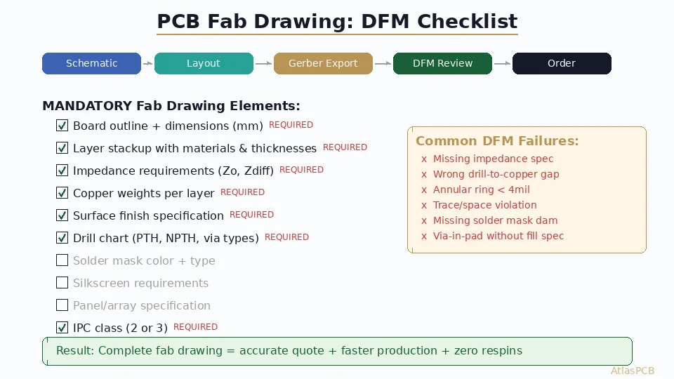
Before submitting your design package, verify these items are present and consistent:
- Impedance table on page 1 with all five required columns filled
- Stackup drawing showing layer materials, thicknesses, and copper weights
- Note stating “Impedance takes priority; fabricator to adjust trace width”
- Measurement standard reference (IPC-TM-650 2.5.5.7)
- Material specification (family or slash-sheet, not hard-coded prepreg part number)
- Coupon requirements for production (optional for prototype)
- No conflicting trace width lock that contradicts impedance target
- Differential pair spacing noted in the impedance table or stackup notes
If your design uses multiple impedance classes on the same layer (e.g., 50 Ohm single-ended and 100 Ohm differential both routing on Layer 3), ensure the table clearly distinguishes them. The fabricator needs to verify that the dielectric height accommodates both targets simultaneously — which it almost always does, since differential impedance is primarily controlled by spacing between traces rather than trace-to-ground distance.
Choosing an Impedance Controlled PCB Manufacturer
A well-specified fab drawing is only half the equation. The other half is choosing a manufacturer with the process controls and equipment to actually deliver controlled impedance consistently. Not all fabricators are equal here — impedance control requires tighter process windows than standard PCB manufacturing.
What distinguishes a qualified impedance controlled PCB manufacturer:
TDR testing equipment and workflow. The manufacturer must own time-domain reflectometry (TDR) equipment calibrated to IPC-TM-650 2.5.5.7 and integrate it into their production flow — not as a special request, but as standard procedure for impedance-controlled orders. Ask whether they test every panel or only sample panels.
Dielectric thickness control. Impedance is a function of trace geometry and dielectric height. A manufacturer with ±10% dielectric thickness variation panel-to-panel cannot reliably hold ±5% impedance tolerance. Ask about their prepreg/core thickness capability (good manufacturers hold ±0.5 mil on standard materials).
Field solver correlation data. A strong manufacturer maintains a database correlating their field solver predictions with actual TDR measurements. This means first-pass impedance accuracy above 95% — fewer engineering queries, fewer coupon failures, and faster delivery.
Coupon design and placement. Test coupons should replicate the actual impedance structures in your design (same layer, same geometry type, same reference plane). Ask whether their coupons are generic (predefined structures) or design-specific (derived from your actual board).
AtlasPCB guarantees ±5% impedance tolerance on all controlled impedance orders, with 100% TDR coupon testing and design-specific coupon generation. Our first-pass impedance yield exceeds 97% — meaning your board ships on time without re-processing.
ATLASPCB
Submit Your Design with Confidence
Our engineering team validates impedance specs as part of every order. No surprises, no re-spins from spec ambiguity.
Upload Design Package ›Reviewed by AtlasPCB Engineering Team — 15+ years in advanced PCB fabrication for RF, HDI, and rigid-flex applications.
Related Reading:
About AtlasPCB — We specialize in complex PCB manufacturing for HDI, RF, and high-reliability applications. Explore our impedance-controlled PCB manufacturing, or get an free engineering DFM review . Every order includes free engineering review. Get your quote.
Reviewed by AtlasPCB Engineering Team — IPC-certified manufacturing specialists with 15+ years of production experience in HDI, RF, and high-reliability PCB fabrication. Content based on factory floor data and real customer design reviews.
- impedance-control
- dfm
- pcb-design
- fabrication
- impedance-controlled-pcb-manufacturer
- controlled-impedance-pcb