· AtlasPCB Engineering · Engineering · 8 min read
Controlled Impedance PCB Pricing: What It Costs and How to Optimize Your Stackup
Detailed breakdown of controlled impedance PCB cost factors — from material selection and dielectric tolerance to TDR testing and coupon design. Learn which impedance specs actually need premium tolerances and where you can save 15-30% by specifying smarter.
Quick Answer: Controlled Impedance Cost Breakdown
| Cost Component | Typical Premium | How to Minimize |
|---|---|---|
| Material tolerance (Dk control) | +5-10% | Use standard FR-4 (Dk 4.2-4.5) |
| Trace width etching control | +5-10% | Specify +/-10% tolerance |
| TDR coupon testing | +$50-150/value/lot | Consolidate to 2-3 impedance values |
| Impedance report | +$30-50/lot | Request only when contractually required |
| Cross-section microsection | +$80-120/lot | Request only for first-article or Class 3 |
| Net cost impact (typical 4L board) | +$2-8/board | Combine all optimization strategies |
For a standard 4-layer board at 100-piece prototype quantity, controlled impedance adds approximately $2-8 per board. At production volumes (1000+ pieces), the per-board premium drops to $0.50-2.00 because testing cost amortizes across more boards.
Why Controlled Impedance Costs More
A conventional PCB without impedance control is manufactured with “best effort” dielectric thickness and trace width. The fabricator targets nominal values but accepts whatever the press and etching processes naturally produce — typically +/-15-20% variation on dielectric thickness and +/-1mil on trace width. This variation is fine for power and low-speed signals but creates unacceptable impedance spread for high-speed transmission lines.
When you specify controlled impedance, the fabricator must tighten process controls at multiple manufacturing stages. The press cycle must produce dielectric thickness within +/-8% (for +/-10% impedance tolerance) or +/-4% (for +/-5% impedance tolerance). Etching must control trace width to +/-0.5mil instead of the standard +/-1.0mil. And every production lot must be verified with time-domain reflectometry (TDR) measurements on dedicated test coupons.
Each of these tighter controls translates directly to cost. The press operation runs at lower stack heights to improve thickness uniformity. Etching requires more frequent bath chemistry monitoring and potentially slower conveyor speeds. And TDR testing requires coupon design, measurement time, and report generation — a dedicated quality step that adds 15-30 minutes of technician time per lot.
IMPEDANCE-CONTROLLED FABRICATION
Stackup Design with Impedance Modeling Included
Tell us your target impedances and we design the stackup — material selection, prepreg combination, and trace geometry calculated for your exact requirements.
Request Stackup Design ›Material Selection: Standard vs Premium Laminates
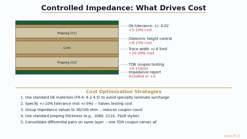
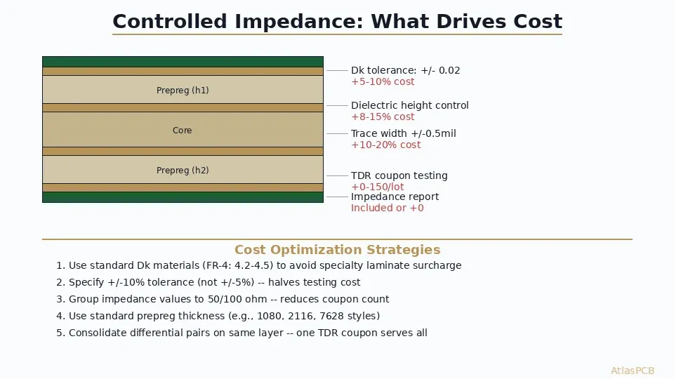
The laminate’s dielectric constant (Dk) tolerance is the foundation of impedance control. Standard FR-4 from major suppliers (Shengyi S1000-2, ITEQ IT-180A, Isola 370HR) ships with Dk specified to +/-0.2 units at 1 GHz. This built-in variation means your 50-ohm target might actually be anywhere from 47 to 53 ohms before you even consider fabrication variation — within +/-10% tolerance for most stackups.
When you specify +/-5% impedance tolerance, the fabricator may need to source material from a specific manufacturer lot with tighter Dk variation, or use a premium laminate grade with Dk tolerance of +/-0.05 (such as Isola I-Tera MT40 or Panasonic Megtron 6). These specialty laminates cost 2-5x more than standard FR-4 and have longer lead times. For most designs below 5 GHz, standard FR-4 with +/-10% impedance tolerance gives you a perfectly functional controlled-impedance board at standard material pricing.
The prepreg style directly impacts cost through material availability. Standard styles (1080 at 2.6mil cured, 2116 at 4.5mil cured, 7628 at 7.0mil cured) are stocked in large quantities and priced as commodity materials. When your stackup calculator calls for a 3.2mil dielectric spacing that requires a non-standard prepreg combination, the fabricator must either special-order material or use multiple plies of thin prepreg — both adding cost and lead time.
The cost-smart approach: design your impedance targets around standard prepreg thicknesses rather than forcing prepreg selection to match arbitrary impedance values. A 50-ohm microstrip on standard 2116 prepreg requires approximately 4.8mil trace width. If your design rule allows 4.8mil traces (rounded to 5mil is even better), you get impedance control at standard material pricing.
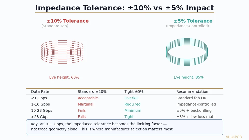
Tolerance Specification: +/-5% vs +/-10%
The impedance tolerance you specify has an outsized impact on fabrication cost because it cascades through multiple process stages. Here is what each tolerance level actually demands:
At +/-10% tolerance, the fabricator needs dielectric thickness within +/-8%, trace width within +/-0.8mil, and TDR readings within +/-10% of target on the coupon. This is achievable with standard press recipes, standard etching parameters, and single-point TDR measurement. Most fabricators handle this level routinely with standard pricing.
At +/-5% tolerance, dielectric thickness must be within +/-4%, trace width within +/-0.4mil, and TDR readings within +/-5%. This requires dedicated press monitoring (often fewer panels per press load for better uniformity), tighter etching process control (slower line speed, more frequent chemistry checks), and more TDR measurement points per coupon. The combined process impact typically adds 15-25% over standard impedance-controlled pricing.
The engineering question is: does your design actually need +/-5%? For most digital interfaces (DDR4/5, PCIe Gen4/5, USB 3.x, Ethernet to 25G), the channel loss budget easily accommodates +/-10% impedance variation. The reflections caused by +/-10% impedance mismatch create approximately -26 dB return loss — well within the noise floor for these protocols. Reserve +/-5% for RF circuits above 6 GHz and 56+ Gbps PAM4 channels where every 0.1 dB of return loss matters.
SIGNAL INTEGRITY EXPERTISE
Not Sure What Tolerance You Need?
Our SI engineers review your interface speeds and recommend the minimum impedance tolerance that meets your performance requirements — saving you from over-specifying.
Get Stackup Recommendation ›TDR Testing and Coupon Strategy
Time-domain reflectometry testing is the verification step that confirms your fabricated board actually meets the impedance specification. Each unique impedance value in your design requires a dedicated test coupon — a set of calibrated transmission lines built into the panel border and measured before the panel is routed into individual boards.
The cost of TDR testing scales linearly with the number of unique impedance values. A design with three impedance values (50 ohm single-ended, 90 ohm differential, 100 ohm differential) requires three separate coupons, three measurement setups, and three entries in the impedance report. Each additional value adds approximately $50-150 per lot in testing cost at most fabricators.
The optimization strategy is consolidation. Can your 85-ohm differential pairs be redesigned as 100-ohm with adjusted termination? Can your 55-ohm single-ended nets be standardized to 50-ohm? Every impedance value you eliminate saves one coupon and one test cycle per production lot. Most high-speed designs can be built around just two values: 50 ohm single-ended and 100 ohm differential. This dual-impedance approach is universally supported, minimizes coupon count, and uses standard trace/space geometries that every fabricator is comfortable producing.
For production volumes, also consider whether you need full TDR testing on every lot or only on the first article. Many fabricators offer “first article + SPC” programs where they fully characterize the first production lot, then monitor process parameters statistically on subsequent lots without measuring every panel. This can reduce ongoing testing cost by 60-80% after process capability is demonstrated.
Stackup Optimization for Cost
The most cost-effective approach to impedance-controlled PCB design is to design your stackup around commercially available materials rather than forcing custom material combinations. Here is a practical optimization workflow:
Start with your fabricator’s standard stackup offerings. Most fabricators publish “standard stackup” documents for 4, 6, and 8-layer boards using their most economical materials. These stackups use stocked prepreg styles at standard thicknesses, have well-characterized Dk values from years of production data, and can be pressed with standard recipes on existing tooling. Designing to these predefined stackups eliminates engineering NRE and reduces lead time.
If your required impedance does not match the standard stackup’s natural impedance, adjust trace width rather than dielectric thickness. It is far cheaper for the fabricator to etch a slightly different trace width (which requires no material change) than to source non-standard prepreg thickness. A 2-mil adjustment in trace width costs nothing extra in fabrication; a non-standard prepreg thickness might add $200-500 in material premium and 3-5 days lead time.
Group your signal integrity requirements by layer. Put all same-impedance signals on the same layer wherever possible. This allows the fabricator to optimize one layer pair’s dielectric precisely rather than needing tight tolerance on every dielectric layer in the stackup. Layers without impedance-critical signals can run at standard (looser) tolerance, reducing overall process difficulty.
ATLASPCB
Impedance-Controlled Boards at Competitive Pricing
Standard stackups for 50/100 ohm from 4 to 30 layers. +/-10% tolerance standard, +/-5% available. TDR report included with every impedance-controlled order.
Get Impedance Board Quote ›Related Reading:
About AtlasPCB — We specialize in complex PCB manufacturing for HDI, RF, and high-reliability applications. Explore our impedance-controlled PCB manufacturing, or get an instant online PCB quote . Every order includes free engineering review. Get your quote.
Reviewed by AtlasPCB Engineering Team — IPC-certified manufacturing specialists with 15+ years of production experience in HDI, RF, and high-reliability PCB fabrication. Content based on factory floor data and real customer design reviews.
- pcb
- impedance-control
- pricing
- signal-integrity
- stackup