· Engineering · 7 min read
How to Specify Impedance Control on Your PCB Fab Drawing
Complete guide to specifying controlled impedance on PCB fabrication drawings. Includes impedance table format, tolerance callouts, coupon requirements, and common mistakes that cause DFM rejections.
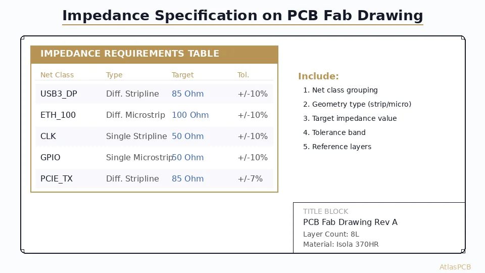
Quick Reference: Impedance Table Format
Your fab drawing needs this table (at minimum):
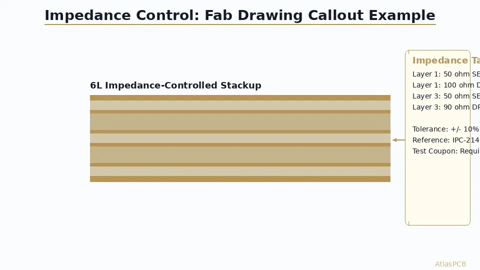
| Layer | Type | Target (ohm) | Width (mil) | Space (mil) | Ref Layer | Tolerance |
|---|---|---|---|---|---|---|
| L1 | Single-ended | 50 | 5.0 | — | L2 (GND) | +/-10% |
| L1 | Differential | 100 | 4.5 | 5.5 | L2 (GND) | +/-10% |
| L3 | Single-ended | 50 | 4.8 | — | L2, L4 (GND) | +/-10% |
| L3 | Differential | 90 | 4.0 | 5.0 | L2, L4 (GND) | +/-10% |
Notes below table:
- Reference standard: IPC-2141A
- Test method: TDR per IPC-TM-650 2.5.5.7
- Coupon: Required on each production panel
- Dk source: Manufacturer’s typical value at target frequency
Why This Matters: The $5,000 Rework Story
A missing or ambiguous impedance callout is the second most common cause of DFM rejection (after insufficient annular ring). Here is what goes wrong:
- No impedance table — Fab assumes no impedance control. Your 50-ohm traces come back at 62 ohms.
- Width specified but not impedance — Fab builds to width, not impedance. Material lot variation shifts Dk, and impedance drifts 8-12%.
- Missing reference layer — In an asymmetric stackup, the fab guesses wrong. Differential pairs come back at 85 ohms instead of 100.
- Over-tight tolerance — Specifying +/-5% on a standard FR-4 build increases cost 30-40% and extends lead time.
Step-by-Step: Adding Impedance Control to Your Fab Package
Step 1: Identify Which Nets Need Control
Not every trace needs impedance control. Focus on:
- USB 2.0/3.x differential pairs (90 ohm)
- PCIe lanes (85 or 100 ohm differential)
- DDR4/5 data/address (40-50 ohm SE, depends on topology)
- Ethernet RGMII/SGMII (100 ohm differential)
- RF transmission lines (50 ohm microstrip or GCPW)
- HDMI/DisplayPort (100 ohm differential)
- Any signal above 100 MHz or with rise time under 1 ns
Step 2: Determine Trace Geometry
Use a field solver (Polar Si9000, Saturn PCB Toolkit, or your EDA’s built-in solver) to calculate initial dimensions:
Inputs needed:
- Target impedance (from interface standard)
- Dielectric constant (from laminate datasheet at your frequency)
- Copper weight (determines trace thickness after plating)
- Prepreg/core thickness (from your stackup)
Key formula relationships:
- Wider trace = lower impedance
- Thicker dielectric = higher impedance
- Higher Dk = lower impedance
- Differential: closer spacing = lower differential impedance
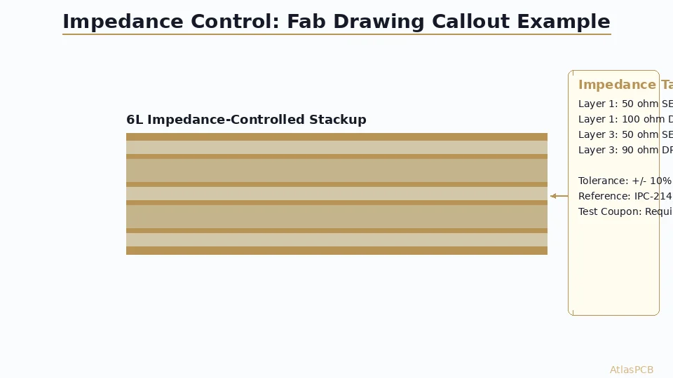
Step 3: Build the Impedance Table
For each controlled impedance class on your board:
IMPEDANCE CONTROL REQUIREMENTS
Reference: IPC-2141A
Test: TDR per IPC-TM-650 2.5.5.7

Class 1: 50 ohm single-ended microstrip
  Layer: L1, L8
  Reference: Adjacent ground plane
  Width: 4.8 mil (nominal)
  Tolerance: +/- 10%

Class 2: 100 ohm differential microstrip
  Layer: L1, L8
  Reference: Adjacent ground plane
  Width: 4.0 mil, Space: 5.5 mil (nominal)
  Tolerance: +/- 10%

Class 3: 50 ohm single-ended stripline
  Layer: L3, L6
  Reference: L2 (GND) and L4 (GND)
  Width: 4.2 mil (nominal)
  Tolerance: +/- 10%

NOTES:
- Widths are nominal. Fab may adjust +/- 0.5 mil
  to meet impedance target on actual materials.
- Impedance value is the CONTROLLING dimension.
- Coupon testing required on each production panel.
IMPEDANCE EXPERTISE
Unsure About Your Stackup? We Run the Sims.
Upload your constraints — we model impedance with Polar Si9000 and return an optimized stackup within 24 hours. No charge for prototype orders.
Submit Stackup for Review ›Common Mistakes That Cause Rejections
Mistake 1: Specifying Impedance Without a Stackup
If you send Gerbers with “50 ohm controlled impedance” but no stackup definition, the fab must guess your dielectric thicknesses. Result: they call you to clarify, adding 2-3 days to your timeline.
Fix: Always include a stackup drawing with:
- Layer sequence and function (signal/ground/power)
- Dielectric thickness per layer (or at minimum, total board thickness target)
- Copper weight per layer
- Material callout (FR-4 Tg170, Megtron 6, etc.)
Mistake 2: Conflicting Width and Impedance Specs
Designers sometimes lock trace width in CAD at 5.0 mil AND specify 50 ohms. But 50 ohms on the actual production material might require 4.7 mil. If both are hard requirements, the fab cannot satisfy both.
Fix: State clearly: “Impedance is controlling dimension. Fab may adjust trace width +/-0.5 mil to achieve target impedance on production material.”
Mistake 3: Not Accounting for Plating
Outer-layer traces get 0.5-1.0 mil of copper added during electroplating. A trace drawn at 5.0 mil in CAD becomes 5.5-6.0 mil after plating. This reduces impedance by 3-8%.
Fix: Your field solver model should include final plated thickness (base copper + plating). Most fabs pre-compensate, but you should note “widths are pre-etch” or “widths are finished” on your drawing.
Mistake 4: Specifying +/-5% on Standard FR-4
Standard FR-4 has Dk tolerance of +/-0.15 (on a Dk of 4.2-4.6). Combined with prepreg thickness variation (+/-0.5 mil), achieving +/-5% impedance requires:
- Cherry-picking material lots
- Tighter etch control
- More coupons per panel
- Lower yield
Cost impact: +/-5% tolerance adds 25-40% to board cost vs +/-10%.
When +/-5% is justified:
- 112G PAM4 channels (56+ GBd)
- RF filter networks with tight passband specs
- Test fixtures requiring known reference impedance
CONTROLLED IMPEDANCE
TDR-Verified on Every Production Panel
AtlasPCB includes impedance coupon testing on all controlled-impedance builds. Test reports delivered with shipment.
View Our Capabilities ›Impedance by Interface Standard
Quick reference for common digital interfaces:
| Interface | Impedance | Type | Typical Width (outer, FR-4 Tg170) |
|---|---|---|---|
| USB 2.0 | 90 ohm | Differential | 5.0 / 5.5 mil (w/s) |
| USB 3.x/4 | 85 ohm | Differential | 4.5 / 5.0 mil (w/s) |
| PCIe Gen3-5 | 85 ohm | Differential | 4.5 / 5.0 mil (w/s) |
| PCIe Gen6 | 85 ohm | Differential | 4.0 / 5.0 mil (Megtron 6) |
| DDR4 | 40 ohm SE | Single-ended | 6.0-7.0 mil |
| DDR5 | 40 ohm SE | Single-ended | 5.5-6.5 mil |
| HDMI 2.1 | 100 ohm | Differential | 4.0 / 6.0 mil (w/s) |
| 10G Ethernet | 100 ohm | Differential | 4.5 / 5.5 mil (w/s) |
| 50 ohm RF | 50 ohm | Single-ended | 8.0-10.0 mil (microstrip) |
Note: These widths are approximate for a typical 4-layer stackup on 1.6mm FR-4 with 1080 prepreg over ground. Your actual stackup will differ.
HIGH-SPEED DESIGN
PCIe Gen5, DDR5, USB4 — We Build Them All
Min trace/space 3/3mil, impedance tolerance to +/-5%. Upload your design for a stackup recommendation matched to your interfaces.
Upload Design ›Checklist Before Sending to Fab
Use this checklist every time you release a controlled-impedance design:
- Impedance table on fab drawing with layer, value, type, width, spacing, reference, tolerance
- Stackup drawing with dielectric thicknesses and material callout
- Clear note: “Impedance is controlling dimension, width is nominal”
- Copper weight specified for each layer
- Board thickness tolerance stated
- Coupon requirement noted (production vs prototype)
- Test method referenced (IPC-TM-650 2.5.5.7)
- Surface finish called out (affects outer layer trace geometry due to plating)
- Via structure specified (especially for stripline layers — stubs affect impedance)
ATLASPCB
Ready to Order? We Validate Your Impedance Specs.
Every impedance-controlled order gets a pre-production stackup simulation. If something does not match, we flag it before manufacturing starts.
Get Instant Quote ›Related Reading:
About AtlasPCB — We specialize in complex PCB manufacturing for HDI, RF, and high-reliability applications. Explore our impedance-controlled PCB manufacturing, or get an free engineering DFM review . Every order includes free engineering review. Get your quote.
Reviewed by AtlasPCB Engineering Team — IPC-certified manufacturing specialists with 15+ years of production experience in HDI, RF, and high-reliability PCB fabrication. Content based on factory floor data and real customer design reviews.
- impedance-control
- dfm
- pcb-fabrication
- engineering