· AtlasPCB Engineering · Engineering · 8 min read
PCB Trace Width and Current Capacity: IPC-2152 Design Guide
A practical guide to PCB trace width sizing for current capacity using IPC-2152. Covers internal and external traces, temperature rise calculations, thermal relief design, and high-current PCB layout techniques for power delivery applications.
One of the most fundamental PCB design tasks is sizing copper traces to carry the required current without excessive temperature rise. Under-sized traces cause reliability failures from overheating; over-sized traces waste board space. This guide covers the IPC-2152 standard for trace current capacity, practical design tables, and high-current layout techniques.
IPC-2152: The Modern Standard
History
PCB trace current capacity was historically determined using charts from IPC-2221 (originally from MIL-STD-275), based on limited testing conducted at the National Bureau of Standards (NBS) in the 1950s. These charts were conservative for external traces and often non-conservative for internal traces.
IPC-2152, published in 2009 and titled “Standard for Determining Current Carrying Capacity in Printed Board Design,” replaced the IPC-2221 charts with data from modern testing under controlled conditions. Key improvements:
- Tested boards with realistic construction (multilayer, FR-4, with planes)
- Separate data for external (outer) and internal (inner) traces
- Correction factors for copper weight, board thickness, and environment
- Data for traces adjacent to copper planes
Key Principles
- Temperature rise, not absolute temperature: IPC-2152 specifies current capacity for a given temperature rise above ambient (typically 10°C, 20°C, or 30°C rise).
- Thermal equilibrium: The trace reaches a steady-state temperature where heat generated (I²R) equals heat dissipated (conduction, convection, radiation).
- Cross-sectional area matters: Current capacity is fundamentally related to the copper cross-sectional area (width × thickness), not width alone.
- Environment matters: An internal trace surrounded by dielectric dissipates heat differently than an external trace exposed to air.
Current Capacity Tables
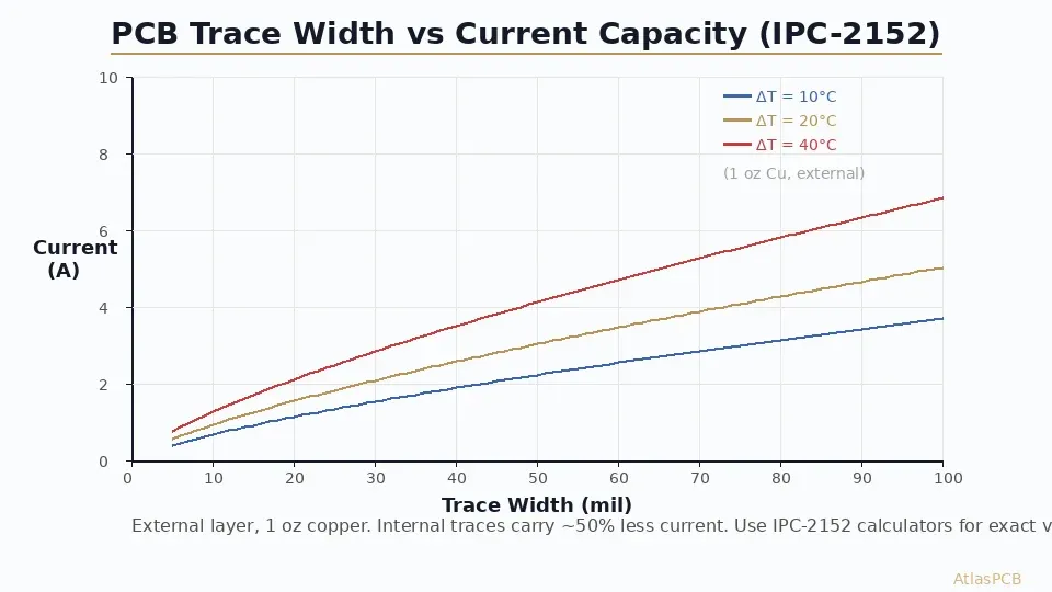
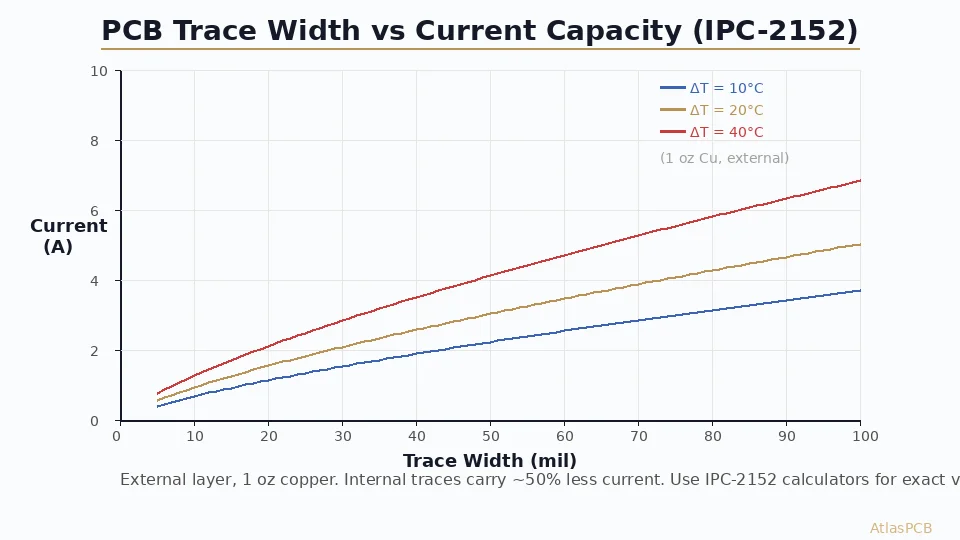
External Traces (Outer Layer)
The following table shows approximate current capacity for external (outer layer) traces on a standard FR-4 multilayer board:
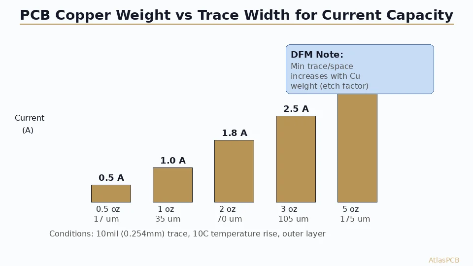
1 oz copper (35 µm / 1.4 mil):
| Trace Width (mil) | Trace Width (mm) | 10°C Rise | 20°C Rise | 30°C Rise | 40°C Rise |
|---|---|---|---|---|---|
| 5 | 0.127 | 0.6 A | 0.8 A | 1.0 A | 1.1 A |
| 10 | 0.254 | 1.0 A | 1.4 A | 1.7 A | 1.9 A |
| 15 | 0.381 | 1.3 A | 1.9 A | 2.3 A | 2.6 A |
| 20 | 0.508 | 1.7 A | 2.3 A | 2.8 A | 3.2 A |
| 30 | 0.762 | 2.2 A | 3.1 A | 3.8 A | 4.3 A |
| 50 | 1.270 | 3.2 A | 4.5 A | 5.5 A | 6.2 A |
| 75 | 1.905 | 4.2 A | 5.9 A | 7.2 A | 8.2 A |
| 100 | 2.540 | 5.1 A | 7.1 A | 8.7 A | 10.0 A |
| 150 | 3.810 | 6.6 A | 9.3 A | 11.4 A | 13.0 A |
| 200 | 5.080 | 8.0 A | 11.2 A | 13.7 A | 15.7 A |
2 oz copper (70 µm / 2.8 mil):
| Trace Width (mil) | Trace Width (mm) | 10°C Rise | 20°C Rise | 30°C Rise | 40°C Rise |
|---|---|---|---|---|---|
| 10 | 0.254 | 1.5 A | 2.1 A | 2.6 A | 2.9 A |
| 20 | 0.508 | 2.5 A | 3.5 A | 4.3 A | 4.9 A |
| 30 | 0.762 | 3.4 A | 4.8 A | 5.8 A | 6.6 A |
| 50 | 1.270 | 4.9 A | 6.9 A | 8.4 A | 9.6 A |
| 100 | 2.540 | 7.8 A | 10.9 A | 13.4 A | 15.3 A |
| 200 | 5.080 | 12.3 A | 17.2 A | 21.1 A | 24.1 A |
Internal Traces (Inner Layer)
Internal traces are less efficient at dissipating heat because they are enclosed in dielectric material. Typical derating: carry 50–70% of external trace current for the same temperature rise.
1 oz copper (35 µm), internal:
| Trace Width (mil) | Trace Width (mm) | 10°C Rise | 20°C Rise | 30°C Rise |
|---|---|---|---|---|
| 10 | 0.254 | 0.6 A | 0.8 A | 1.0 A |
| 20 | 0.508 | 1.0 A | 1.4 A | 1.7 A |
| 30 | 0.762 | 1.4 A | 1.9 A | 2.3 A |
| 50 | 1.270 | 2.0 A | 2.8 A | 3.4 A |
| 100 | 2.540 | 3.2 A | 4.5 A | 5.5 A |
| 200 | 5.080 | 5.1 A | 7.1 A | 8.7 A |
Important notes:
- Values are approximate; use IPC-2152 software or lookup tables for exact values
- Ambient temperature: 25°C (adjust for other ambient conditions)
- Still air (no forced convection); forced air increases capacity significantly
- Values assume isolated traces; adjacent traces carrying current reduce capacity
Correction Factors
Copper Thickness
Current capacity scales approximately with the square root of copper thickness:
I₂ / I₁ ≈ (t₂ / t₁)^0.5
A 2 oz (70 µm) trace carries approximately √2 ≈ 1.41× the current of a 1 oz trace at the same width and temperature rise.
Proximity to Copper Planes
Adjacent copper planes (ground or power) on the next layer significantly improve heat dissipation:
| Dielectric Thickness to Plane | Current Increase |
|---|---|
| 4 mil (100 µm) | +30–40% |
| 8 mil (200 µm) | +20–30% |
| 12 mil (300 µm) | +10–15% |
| No adjacent plane | Baseline |
This is one of the most significant factors. An external trace with a ground plane on the adjacent layer at 100 µm spacing can carry 30–40% more current than the IPC-2152 baseline (which assumes no adjacent plane in the basic charts).
Board Thickness
Thicker boards provide more thermal mass and heat spreading. Correction is typically +5–10% for boards >2 mm thick compared to the baseline.
Ambient Temperature
The temperature rise is above ambient. If ambient is 50°C and maximum copper temperature is 100°C, the allowable rise is only 50°C. Higher ambient temperature does not change the current for a given rise, but it reduces the available rise budget.
Maximum copper temperature guidelines:
- Standard FR-4: 105–130°C (Tg dependent)
- High-Tg FR-4: 150–170°C
- Polyimide: 200°C+
- IPC-2152 test data is valid up to approximately 100°C above ambient
Via Current Capacity
Vias in current paths must also be sized appropriately. A standard plated through-hole via carries less current than a trace due to its small copper cross-section.
Via Current Estimation
The copper in a via barrel forms a hollow cylinder:
Cross-sectional area = π × D × t
Where D is the drilled hole diameter and t is the plating thickness.
| Via Drill (mm) | Plating (µm) | Cu Area (mm²) | Approx. Current (10°C rise) |
|---|---|---|---|
| 0.20 | 20 | 0.0126 | 0.7 A |
| 0.25 | 25 | 0.0196 | 1.0 A |
| 0.30 | 25 | 0.0236 | 1.2 A |
| 0.40 | 25 | 0.0314 | 1.5 A |
| 0.50 | 25 | 0.0393 | 1.8 A |
Paralleling Vias
For currents exceeding single-via capacity, use multiple vias in parallel:
| Required Current | Via Size | Number of Vias | Array Configuration |
|---|---|---|---|
| 3 A | 0.3 mm | 3–4 | Line or 2×2 grid |
| 5 A | 0.3 mm | 5–6 | 2×3 grid |
| 10 A | 0.3 mm | 10–12 | 3×4 grid |
| 20 A | 0.4 mm | 15–20 | 4×5 grid |
| 50 A | 0.5 mm | 30–40 | Array with thermal relief |
Current sharing: Vias at the edges of an array carry more current than those in the center (current crowding). Increase via count by 20–30% beyond the simple I/N calculation to account for uneven distribution.
High-Current PCB Design Techniques
Polygon Pours
For currents above 10A, traces become impractically wide. Use copper polygon pours instead:
- Fill entire available area with copper connected to the power net
- Avoid bottlenecks: Ensure the narrowest point in the pour is adequately sized
- Current density mapping: Use power integrity simulation to visualize current density and identify hotspots
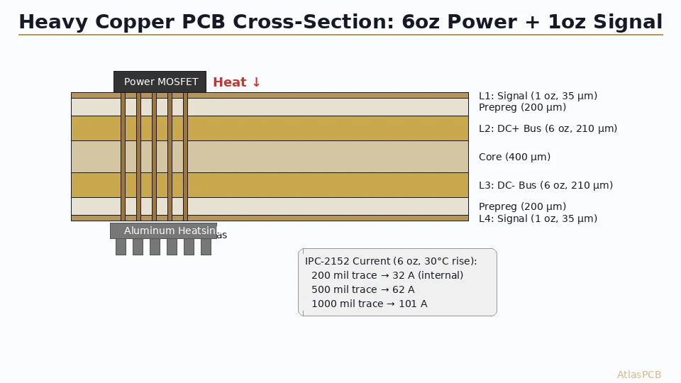
Heavy Copper (2–20 oz)
For extreme current applications (50–200A), heavy copper PCBs use 2 oz to 20 oz copper:
| Copper Weight | Thickness (µm) | Typical Current Range |
|---|---|---|
| 2 oz | 70 | 5–20 A per trace |
| 3 oz | 105 | 10–30 A per trace |
| 4 oz | 140 | 15–40 A per trace |
| 6 oz | 210 | 25–60 A per trace |
| 10 oz | 350 | 50–100 A per trace |
| 20 oz | 700 | 100–200 A per trace |
Heavy copper requires special etching processes and wider trace/space rules. Minimum trace/space at 4 oz is typically 10/10 mil (vs. 3.5/3.5 mil at 1 oz).
Bus Bars and Embedded Copper
For >100A applications, embedded copper bus bars (stamped copper inserts laminated into the PCB) provide the lowest resistance power delivery. These are custom solutions manufactured by specialty fabricators.
Thermal Vias Under Power Components
Components dissipating significant power (voltage regulators, MOSFETs, power inductors) benefit from thermal via arrays connecting the thermal pad to inner copper planes:
- Via diameter: 0.3–0.4 mm
- Via spacing: 1.0–1.2 mm center-to-center (grid)
- Via fill: Copper-filled or plugged with solder (for SMT reflow)
- Target thermal resistance: 15–30°C/W for a 3×3 via array through 1.6 mm board
Practical Design Rules
Minimum Trace Width by Current
Quick reference for 1 oz copper, external trace, 20°C rise:
| Current (A) | Min Trace Width (mil) | Min Trace Width (mm) |
|---|---|---|
| 0.5 | 5 | 0.127 |
| 1.0 | 8 | 0.203 |
| 2.0 | 15 | 0.381 |
| 3.0 | 25 | 0.635 |
| 5.0 | 45 | 1.143 |
| 10.0 | 110 | 2.794 |
| 15.0 | 200 | 5.080 |
| 20.0 | 300+ | 7.620+ |
Design Checklist for Power Traces
- ☐ Calculate required trace width using IPC-2152 for target temperature rise
- ☐ Apply correction factors for copper weight, plane proximity, and ambient temperature
- ☐ Size vias for current capacity (parallel as needed)
- ☐ Check trace width at bottleneck points (between pads, around vias)
- ☐ Verify voltage drop (I × R) is acceptable for voltage-sensitive rails
- ☐ Add thermal relief to power pads if required for assembly (balanced spoke pattern)
- ☐ Review with fabricator for heavy copper or special requirements
Voltage Drop Calculation
For long power traces, voltage drop may be more constraining than temperature rise:
V_drop = I × R = I × (ρ × L) / (w × t)
Where:
- ρ = copper resistivity = 1.72 × 10⁻⁸ Ω·m (at 20°C) or 1.68 µΩ·cm
- L = trace length
- w = trace width
- t = copper thickness
Example: 5A through a 100 mm long, 50 mil (1.27 mm) wide, 1 oz (35 µm) trace:
R = (1.72 × 10⁻⁸ × 0.1) / (1.27 × 10⁻³ × 35 × 10⁻⁶) = 38.7 mΩ
V_drop = 5 × 0.0387 = 0.194 V
For a 3.3V rail, this is 5.9% voltage drop—potentially too high. Solutions: widen the trace, use heavier copper, or shorten the path.
Thermal Simulation
For critical power delivery designs, thermal simulation provides much more accurate results than IPC-2152 tables:
When to Simulate
- Current >10A in any trace
- Board-level thermal budget is tight (constrained enclosure)
- Multiple high-current traces in proximity
- Forced-air or liquid cooling present
- Regulatory or safety certification requirements (UL, IEC)
Simulation Approach
- Import PCB layout into thermal simulation tool (Ansys Icepak, Cadence Celsius, Mentor FloTHERM)
- Define current loads on each power net
- Apply boundary conditions (ambient temperature, airflow, heat sinks)
- Run steady-state thermal analysis to determine copper temperature map
- Iterate trace widths until all copper temperatures are within budget
UL and Safety Considerations
For products requiring UL, CSA, or IEC safety certification:
- UL 796 (printed wiring boards) specifies minimum conductor spacing and width for safety isolation
- IEC 60950 / IEC 62368: Minimum creepage and clearance distances based on voltage and pollution degree
- UL-rated current capacity may differ from IPC-2152 values — always verify with the certifying body
Traces carrying hazardous voltages (>42.4V peak or 60V DC) must meet minimum spacing requirements regardless of current. See our [PCB design rules guide]/blog/pcb-design-rules-trace-width-spacing/) for spacing details.
Conclusion
PCB trace width sizing is a fundamental design task with significant reliability implications. IPC-2152 provides the modern, data-driven framework for determining current capacity, replacing outdated IPC-2221 charts. By understanding the key factors—copper cross-section, temperature rise, plane proximity, and via current sharing—designers can size traces confidently for any current requirement.
For high-current PCB designs, Atlas PCB offers heavy copper capability up to 10 oz, precision copper plating for consistent trace thickness, and DFM review specific to power delivery. Request a quote for your power PCB project.
For related topics, see our guides on [PCB design rules for trace width and spacing]/blog/pcb-design-rules-trace-width-spacing/), [stackup design]/blog/pcb-stackup-design-guide/), and [multilayer PCB manufacturing]/blog/multilayer-pcb-manufacturing-process-explained/).
Further Reading
- [High-Multilayer FR4 vs Standard FR4: When to Upgrade Material Grade]/blog/high-multilayer-fr4-vs-standard-fr4/)
- [Multilayer PCB Stackup Design Guide: 8 to 30+ Layers Step by Step]/blog/multilayer-pcb-stackup-design-guide/)
- [PCB DFM Checklist: 50 Points to Review Before Sending Gerbers]/blog/pcb-dfm-checklist/)
- [PCB Thermal Management: Heat Dissipation Techniques for Reliable Electronics]/blog/pcb-thermal-management/)
- [Heavy Copper PCB: Design Rules, Manufacturing Limits, and Thermal Management]/blog/heavy-copper-pcb/)
About AtlasPCB — We specialize in complex PCB manufacturing for HDI, RF, and high-reliability applications. Explore our aluminum and metal-core PCB services, or get an full PCB manufacturing capabilities . Every order includes free engineering review. Get your quote.
Reviewed by AtlasPCB Engineering Team — IPC-certified manufacturing specialists with 15+ years of production experience in HDI, RF, and high-reliability PCB fabrication. Content based on factory floor data and real customer design reviews.
- trace width
- current capacity
- IPC-2152
- power PCB
- thermal design