· AtlasPCB Engineering · Engineering · 11 min read
Controlled Impedance PCB Design: Stack-Up Calculations, Tolerance Analysis, and Manufacturing Guide
Master controlled impedance PCB design from first principles. Learn impedance calculation formulas, stack-up optimization for 50Ω/100Ω targets, dielectric material selection, trace geometry rules, TDR measurement, and manufacturing tolerance budgets for high-speed digital and RF applications.
Introduction: Why Impedance Control Matters in Modern PCB Design
Every signal on a PCB is a traveling wave. When a signal encounters a change in characteristic impedance — a trace that widens, narrows, or transitions between layers — part of the wave reflects back toward the source. These reflections corrupt signal integrity, create timing uncertainty, and at high data rates, make reliable communication impossible.
Controlled impedance means designing and manufacturing PCB traces to maintain a specific characteristic impedance (typically 50Ω or 100Ω differential) within a defined tolerance. It’s not optional for:
- High-speed digital: PCIe Gen 5/6, DDR5, USB4, Ethernet 25G+
- RF/microwave: Antenna feeds, filter networks, amplifier matching
- SerDes interfaces: 56/112 Gbps PAM4 signaling
- Automotive radar: 77 GHz FMCW front-end PCBs
This guide covers controlled impedance from first principles through manufacturing, giving you the knowledge to design boards that work at the bench — not just in simulation.
Impedance Fundamentals: The Physics
Characteristic impedance (Z₀) is determined by the distributed inductance and capacitance per unit length of a transmission line:
Z₀ = √(L/C)Where:
- L = inductance per unit length (nH/mm), determined by trace geometry and return path distance
- C = capacitance per unit length (pF/mm), determined by trace geometry, dielectric properties, and reference plane distance
For PCB traces, this translates to three physical parameters you can control:
- Trace width (W): Wider = lower impedance (more capacitance, less inductance)
- Dielectric height (H): Taller = higher impedance (less capacitance)
- Dielectric constant (Dk): Higher Dk = lower impedance (more capacitance)
And one parameter that has secondary influence: 4. Copper thickness (T): Thicker copper slightly reduces impedance (more capacitance at edges)
Transmission Line Structures on PCBs
PCBs support several impedance-controlled structures:
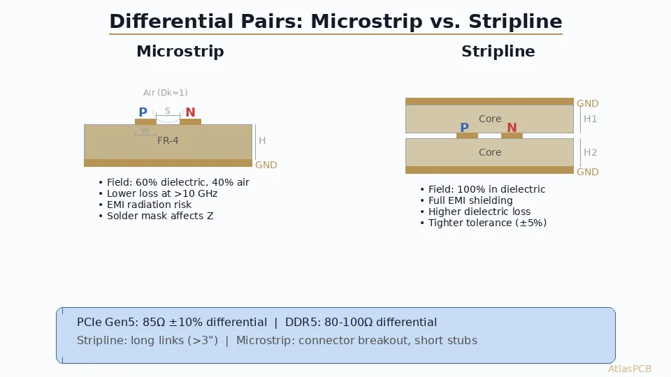
Microstrip (Outer Layer)
The most common structure: a trace on an outer layer referenced to a single ground plane below.
Approximate formula (empirical, ±5% accuracy for W/H > 0.5):
Z₀ ≈ (87 / √(Dk_eff + 1.41)) × ln(5.98H / (0.8W + T))Where Dk_eff accounts for the partial-air, partial-dielectric environment of microstrip.
Typical 50Ω microstrip geometries:
| Dielectric Height (H) | Trace Width (W) | Dk | Copper (T) |
|---|---|---|---|
| 3.5 mil | 4.0 mil | 4.2 | 0.5 oz (0.7mil) |
| 4.0 mil | 4.8 mil | 4.2 | 0.5 oz |
| 4.0 mil | 5.5 mil | 3.7 | 0.5 oz |
| 5.0 mil | 6.5 mil | 4.2 | 1.0 oz |
| 4.0 mil | 7.5 mil | 3.0 | 0.5 oz |
Embedded Microstrip (Outer Layer with Solder Mask)
Real PCBs have solder mask over outer-layer traces. This increases effective Dk and reduces impedance by 2-8%. Always include solder mask in calculations.
Stripline (Inner Layer)
A trace between two reference planes — the “shielded” configuration:
Approximate formula:
Z₀ ≈ (60 / √Dk) × ln(4B / (0.67π(0.8W + T)))Where B = total distance between the two reference planes.
Typical 50Ω stripline geometries:
| Total Dielectric (B) | Trace Width (W) | Dk | Copper (T) |
|---|---|---|---|
| 10.0 mil | 4.0 mil | 4.2 | 0.5 oz |
| 12.0 mil | 5.0 mil | 4.2 | 0.5 oz |
| 8.0 mil | 3.5 mil | 3.7 | 0.5 oz |
| 14.0 mil | 6.0 mil | 4.2 | 1.0 oz |
Asymmetric stripline (trace not centered between planes) is common in real stackups. Use a field solver for accurate results — formulas assume centered placement.
Edge-Coupled Differential Pair
For 100Ω differential impedance (most common for high-speed digital):
The trace spacing (S) and width (W) together determine differential impedance:
Z_diff ≈ 2 × Z_odd ≈ 2 × Z₀ × (1 - 0.48 × e^(-0.96 × S/H))Tighter coupling (smaller S) reduces differential impedance and improves common-mode noise rejection.
Typical 100Ω differential pair geometries (microstrip):
| H (mil) | W (mil) | S (mil) | Dk | Z_diff |
|---|---|---|---|---|
| 4.0 | 4.0 | 5.0 | 4.2 | ~100Ω |
| 4.0 | 3.5 | 4.0 | 4.2 | ~100Ω |
| 3.5 | 3.5 | 5.5 | 4.2 | ~100Ω |
| 4.0 | 4.5 | 7.0 | 3.7 | ~100Ω |
Broadside-Coupled Differential Pair
Traces on adjacent layers, vertically aligned. Less common but useful for ultra-tight routing where horizontal space is limited. Requires careful manufacturing control of registration between layers.
Stack-Up Design for Impedance Control
The PCB stackup is where impedance control starts. A well-designed stackup makes impedance targets achievable with standard trace widths; a poor stackup forces exotic geometries or unmanufacturable tolerances.
Stack-Up Design Principles
Principle 1: Consistent dielectric thickness on impedance layers
Every impedance-controlled layer needs a predictable, controlled dielectric height to its reference plane. This means:
- Use single-ply prepreg (not multi-ply) for impedance-critical dielectric layers
- Specify prepreg types with low thickness variation (±10% → ±0.4mil on 4mil nominal)
- Maintain uniform copper coverage on adjacent layers (affects pressed prepreg thickness)
Principle 2: Reference planes must be continuous
A trace over a split reference plane has undefined impedance at the split boundary. For controlled impedance:
- Dedicate full ground planes adjacent to impedance layers
- Never route signals across plane splits
- If plane splits are unavoidable, add stitching capacitors at crossings
Principle 3: Symmetric stackup for manufacturing
Asymmetric stackups warp during lamination. Even if electrically acceptable, maintain symmetry for flat panels that yield reliable impedance.
Example 6-Layer Impedance-Controlled Stack-Up
Layer 1 (Signal/Microstrip): 50Ω SE / 100Ω Diff
  ├─ Prepreg: 1080 × 1 ply (3.5mil pressed), Dk=4.2
Layer 2 (Ground Plane): Reference for L1
  ├─ Core: 8.0mil, Dk=4.2
Layer 3 (Signal/Stripline): 50Ω SE / 100Ω Diff
  ├─ [Symmetry center]
Layer 4 (Signal/Stripline): 50Ω SE / 100Ω Diff
  ├─ Core: 8.0mil, Dk=4.2
Layer 5 (Power/Ground): Reference for L6
  ├─ Prepreg: 1080 × 1 ply (3.5mil pressed), Dk=4.2
Layer 6 (Signal/Microstrip): 50Ω SE / 100Ω Diff
Impedance results (using field solver):
- L1/L6 microstrip: W=4.5mil → 50.2Ω (target: 50 ±10%)
- L1/L6 differential: W=4.0mil, S=5.0mil → 99.8Ω (target: 100 ±10%)
- L3/L4 stripline: W=4.2mil → 50.5Ω
- L3/L4 differential: W=3.8mil, S=5.0mil → 100.3Ω
Need Expert Stack-Up Review?
AtlasPCB's engineering team reviews your stackup and provides impedance simulation — free with every quote
Submit Your Stack-Up →Dielectric Material Selection
Material choice directly impacts impedance achievability and consistency:
FR-4 (Standard and High-Speed Grades)
| Material | Dk (@ 1GHz) | Dk Tolerance | Df (@ 1GHz) | Best For |
|---|---|---|---|---|
| Standard FR-4 (IT-180A) | 4.2-4.5 | ±5-8% | 0.018-0.022 | ≤3 Gbps, cost-sensitive |
| Mid-loss (Panasonic R-1566) | 3.8-4.0 | ±3-5% | 0.010-0.013 | 3-10 Gbps, balanced |
| Low-loss (Megtron 6) | 3.4-3.7 | ±2-3% | 0.004-0.006 | 10-56 Gbps, premium |
| Ultra-low-loss (Megtron 7) | 3.3-3.4 | ±2% | 0.002-0.003 | 56-112 Gbps, data center |
Controlled-Dk Materials
For tight impedance tolerance (±5% or better), standard FR-4’s Dk variation is often the limiting factor. Controlled-Dk materials offer:
- Batch-to-batch Dk consistency within ±2%
- Published Dk at multiple frequencies (important: Dk decreases with frequency)
- Documented Dk at your operating temperature
- Fiber-weave-compensated constructions (spread glass) for reduced Dk spatial variation
RF Materials
For RF/microwave PCBs requiring impedance control above 5 GHz:
| Material | Dk | Dk Tolerance | Frequency Range |
|---|---|---|---|
| Rogers RO4003C | 3.38 | ±0.05 | DC-40 GHz |
| Rogers RO4350B | 3.48 | ±0.05 | DC-40 GHz |
| Isola Astra MT77 | 3.0 | ±0.04 | DC-77 GHz |
| Rogers RT/duroid 5880 | 2.2 | ±0.02 | DC-77 GHz |
The extremely tight Dk tolerance of RF materials (±1-2%) enables impedance control to ±3% or better — critical for filter and matching network applications.
Manufacturing Tolerance Budget
Understanding what manufacturing can achieve helps set realistic impedance targets:
Trace Width Tolerance
| Process | Width Tolerance | Impact on 50Ω |
|---|---|---|
| Standard etch (1oz Cu) | ±1.0 mil | ±3-5Ω |
| Controlled etch (0.5oz Cu) | ±0.5 mil | ±1.5-2.5Ω |
| mSAP (semi-additive) | ±0.3 mil | ±0.8-1.5Ω |
Thinner copper etches more consistently. For tight impedance, consider:
- Starting with 0.5oz (17µm) copper for signal layers
- Plating up to final thickness after etch (better width control)
- Specifying pattern plating rather than panel plating
Dielectric Thickness Tolerance
| Construction | Thickness Tolerance | Impact on 50Ω |
|---|---|---|
| Multi-ply prepreg (e.g., 3×1080) | ±15% | ±3-5Ω |
| Single-ply prepreg (e.g., 1×2116) | ±10% | ±2-3Ω |
| Core material | ±8% | ±1.5-2.5Ω |
| Controlled layup (single-ply, spec’d) | ±5% | ±1-1.5Ω |
Dk Variation
| Material Type | Dk Variation | Impact on 50Ω |
|---|---|---|
| Standard FR-4 | ±5-8% | ±1.5-3Ω |
| Controlled-Dk FR-4 | ±2-3% | ±0.5-1.5Ω |
| RF laminate (Rogers) | ±1-2% | ±0.3-0.8Ω |
Combined Tolerance (RSS Method)
Using root-sum-square combination of independent variables:
Standard process on FR-4:
- Trace width: ±2.5Ω
- Dielectric height: ±2.0Ω
- Dk variation: ±1.5Ω
- RSS total: ±3.5Ω (±7% on 50Ω) ✓ Achievable
Controlled process on Megtron 6:
- Trace width: ±1.5Ω
- Dielectric height: ±1.0Ω
- Dk variation: ±0.8Ω
- RSS total: ±2.0Ω (±4% on 50Ω) ✓ Premium achievable
Impedance Test Coupons
Manufacturers verify impedance using TDR (Time Domain Reflectometry) measurement of dedicated test coupons on each production panel:
Coupon Design
- Test traces replicate the actual impedance structures in the design
- Coupons include microstrip and stripline variants per layer
- Standard coupon length: 150-200mm (enough for TDR window)
- Include both single-ended and differential pair structures
- Launch pads designed for TDR probe connection (typically SMA or microprobe)
Measurement Method
TDR sends a fast-edge pulse down the test trace and measures the reflected signal:
- Launch compensation removes probe/connector effects
- Measurement window excludes first/last 10mm (launch transition zone)
- Average impedance over the measurement window is reported
- IPC-TM-650, Method 2.5.5.7 defines the standard test procedure
Acceptance Criteria
| Tolerance Spec | Pass Criteria | Typical Application |
|---|---|---|
| ±10% (standard) | 45-55Ω measured | Consumer, IoT, general digital |
| ±7% | 46.5-53.5Ω measured | Telecom, automotive |
| ±5% | 47.5-52.5Ω measured | Aerospace, data center, 56G+ SerDes |
What To Do When Coupons Fail
If impedance coupons measure out-of-spec:
- Check the coupon, not just the result — manufacturing damage, probe contact issues
- Review etch data — measure actual trace width microscopically
- Cross-section analysis — verify dielectric thickness and Dk from coupon
- Determine root cause before re-running (etch, lamination, or material lot issue)
- Negotiate disposition — ±12% on a ±10% spec may be acceptable for prototype lots
Design Rules for Impedance Consistency
Beyond calculating the right geometry, maintaining consistent impedance requires disciplined routing:
Rule 1: Maintain Constant Reference
Never let an impedance-controlled trace cross a reference plane gap or boundary:
- If a power plane has cutouts, route signals around them on the reference ground layer
- When transitioning between layers, place ground vias adjacent to signal vias (return path continuity)
- Anti-pads around signal vias on reference planes should be minimized (standard 20mil clearance)
Rule 2: Keep Trace Width Constant
Any width change creates an impedance discontinuity:
- Avoid necking down between BGA escape channels (maintain width, reduce spacing carefully)
- Pad-to-trace transitions create capacitive loads — use teardrops to smooth the transition
- Length matching serpentines should maintain trace width (no accordion-style width changes)
Rule 3: Control Copper on Adjacent Layers
Copper density on adjacent layers affects pressed prepreg thickness:
- Large copper pours adjacent to impedance layers create thinner dielectric (lower H = lower impedance)
- Void areas (no copper) leave thicker dielectric (higher H = higher impedance)
- Solution: Maintain uniform copper fill on reference planes (add copper fill patterns in void areas)
Rule 4: Via Transitions Need Return Paths
Every via transition creates an impedance discontinuity. Minimize it by:
- Placing ground return vias within 20mil of every signal via
- Using back-drilled or blind vias to reduce stub length (critical above 10GHz)
- Matching via pad size to trace impedance (oversized pads add capacitance)
- Using via models in your signal integrity simulation (not just trace models)
Rule 5: Fiber Weave Awareness
Standard E-glass fiber weave in FR-4 creates spatial Dk variation:
- Glass bundles: Dk ≈ 6.2
- Resin between bundles: Dk ≈ 3.0
- A narrow trace aligned with glass has different impedance than one in resin
Mitigation strategies:
- Use spread-glass or flat-glass constructions for critical layers
- Route traces at angles to the weave (not parallel to warp or fill)
- Use wider traces that average over multiple glass/resin areas
- Specify 1080 or 2116 weave styles (finer glass pattern, less variation)
Common Impedance Design Mistakes
Mistake 1: Using Online Calculators Without Validation
Free online impedance calculators use simplified formulas that assume ideal conditions:
- They don’t account for etch factor (trapezoidal cross-section)
- Solder mask effects are often ignored
- Adjacent trace coupling is not modeled
- Copper roughness effects at high frequency are absent
Solution: Always get your PCB manufacturer’s impedance simulation — they use calibrated models matched to their process data.
Mistake 2: Specifying Impedance Without Layer Assignment
“All signals shall be 50Ω” without specifying which layers are controlled leads to:
- Manufacturer guessing which layers need impedance control
- Cost adders for controlling layers that don’t need it
- Mismatched expectations on which traces are measured
Solution: Specify impedance requirements per layer: “Layer 1 microstrip: 50Ω ±10% (5.0mil trace over 4.0mil dielectric to L2 ground)“
Mistake 3: Ignoring Temperature Effects
Dk changes with temperature:
- FR-4: +400-600 ppm/°C below Tg, +1500-2000 ppm/°C above Tg
- A board operating at 85°C has 2-3% lower impedance than at 25°C measurement
For aerospace/automotive applications with wide temperature ranges, include temperature derating in your impedance budget.
Mistake 4: Not Communicating Stackup to the Manufacturer
Sending Gerber files without a defined stackup forces the manufacturer to guess:
- They may use different prepreg types than your simulation assumed
- Core thicknesses might not match your model
- Dk values at the actual operating frequency may differ
Solution: Submit a detailed stackup drawing or use [IPC-2581 data format]/blog/ipc-2581-digital-twin-pcb-data-exchange/) which embeds stackup specifications in the design data.
Impedance Control in Practice: Application Examples
Example 1: PCIe Gen 5 (32 GT/s)
- Requirement: 85Ω ±7% differential (per PCI-SIG spec)
- Structure: Edge-coupled stripline on inner layers
- Material: Megtron 6 (Dk=3.6, Df=0.004)
- Geometry: W=3.8mil, S=5.0mil, H=4.0mil (each side to reference)
- Key challenge: Maintaining impedance through BGA breakout region
Example 2: DDR5 (4800-6400 MT/s)
- Requirement: 40Ω single-ended data, 80Ω differential clock
- Structure: Microstrip on outer layer (short trace lengths)
- Material: Standard FR-4 adequate (Dk=4.2)
- Geometry: Data W=5.5mil over 3.5mil H; Clock W=4.0mil, S=5.0mil
- Key challenge: Length matching within ±1ps with consistent impedance
Example 3: 77 GHz Automotive Radar
- Requirement: 50Ω microstrip, ±3% tolerance
- Structure: Inverted microstrip (grounded coplanar waveguide)
- Material: Rogers RO3003 (Dk=3.0, ±0.04)
- Geometry: W=8.2mil with coplanar ground gap=4mil on 5mil substrate
- Key challenge: Connector transition and via fencing for mode suppression
Conclusion: Impedance Control Is a System Problem
Controlled impedance isn’t just about calculating the right trace width — it’s a system engineering challenge spanning design, materials, manufacturing, and measurement. Success requires:
- Proper material selection matched to your frequency and tolerance requirements
- Stack-up co-design between your signal integrity team and PCB manufacturer
- Explicit documentation specifying exactly what’s controlled and how it’s verified
- Manufacturing partnership with a fabricator that understands and can deliver your requirements
The trend toward faster data rates (112G, 224G) and higher frequencies (5G mmWave, automotive radar) will only increase the importance of impedance control. Engineers who master these fundamentals today will be well-prepared for tomorrow’s challenges.
Need controlled impedance PCBs manufactured to tight tolerances? Get a quote from AtlasPCB — we provide free impedance simulation, stackup optimization, and TDR-verified production with ±5% tolerance capability.
Further Reading
- [Controlled Impedance PCB Stackup Design: Rules, Calculations, and Manufacturing Tolerances for High-Speed Designs]/blog/controlled-impedance-pcb-stackup-design-rules/)
- [PCB Manufacturer with Engineering Review: Why Human DFM Audit Matters]/blog/pcb-manufacturer-engineering-review/)
- [Aluminum PCB Thermal Design for High-Power LED and Motor Drivers: Material Selection, Stackup, and DFM Guide]/blog/aluminum-pcb-thermal-design-led-motor-driver/)
- [AI Hardware PCB Thermal Management: Advanced Multilayer Stackup Design for 1000W+ Processing Units]/blog/ai-hardware-pcb-thermal-management-multilayer-design/)
- [PCB Manufacturing Process: 15 Steps from Gerber to Finished Board]/blog/pcb-manufacturing-process-15-steps/)
- Rigid PCB Manufacturing
About AtlasPCB — We specialize in complex PCB manufacturing for HDI, RF, and high-reliability applications. Explore our RF and high-frequency PCB services, or get an impedance-controlled PCB manufacturing . Every order includes free engineering review. Get your quote.
Reviewed by AtlasPCB Engineering Team — IPC-certified manufacturing specialists with 15+ years of production experience in HDI, RF, and high-reliability PCB fabrication. Content based on factory floor data and real customer design reviews.
- controlled impedance
- PCB stackup
- signal integrity
- impedance calculation
- microstrip
- stripline
- TDR
- high-speed design
- dielectric constant