· AtlasPCB Engineering · Engineering · 12 min read
PCB Gold Finger Connector Design: Hard Gold Plating, Beveling & IPC-6012 Requirements
Comprehensive engineering guide to PCB gold finger edge connector design covering hard gold plating specifications (30-50μin), nickel underplate requirements, beveling angles, dimensional tolerances, and IPC-6012 Section 3.6 acceptance criteria for PCIe, DIMM, and industrial backplane applications.

PCB Gold Finger Connector Design: Complete Engineering Guide
Gold finger edge connectors remain one of the most demanding PCB features to manufacture correctly. From PCI Express slots to DDR5 DIMM modules, from industrial backplane bus connections to test fixture interfaces, gold finger contacts must deliver reliable, low-resistance electrical connections across hundreds or thousands of insertion-extraction cycles. This guide covers the complete engineering specification for gold finger design, plating, and quality assurance per [IPC standards]/blog/pcb-manufacturing-process/).
Gold Finger Fundamentals
Gold fingers are the exposed copper pads along the edge of a PCB, plated with hard electrolytic gold over a nickel barrier layer. They slide into a mating connector (socket) that uses spring-loaded contacts to establish electrical connections. The gold plating serves three critical functions:
Low contact resistance: Gold’s electrical resistivity (2.44×10⁻⁸ Ω·m) and resistance to oxidation ensure stable contact resistance below 20mΩ across the connector interface life.
Wear resistance: Hard gold alloyed with cobalt (Knoop hardness 130-200 HK) provides a durable contact surface that withstands mechanical abrasion from repeated insertions without significant material loss.
Corrosion protection: Gold is noble—it does not form oxides, sulfides, or other insulating films in normal operating environments, maintaining reliable contact even after years of service.
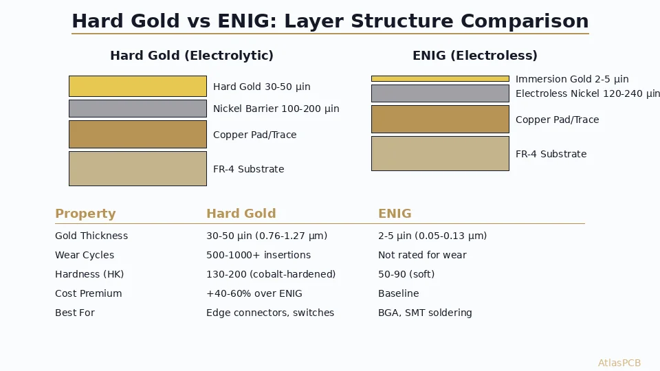
Gold Types: Hard vs. Soft
Understanding the distinction between hard and soft gold is critical for specifying gold fingers correctly:
Hard gold (Type I per ASTM B488 / MIL-G-45204):
- Composition: 99.7% Au + 0.3% Co (most common) or 0.3% Ni
- Hardness: 130-200 HK (Knoop)
- Surface: Matte to semi-bright
- Application: Edge connectors, contact pads, any surface subject to mechanical wear
- Thickness: 30-50μin (0.76-1.27μm) standard; up to 100μin for high-cycle applications
Soft gold (Type III per ASTM B488):
- Composition: 99.99% Au (pure)
- Hardness: 60-90 HK
- Surface: Bright, highly reflective
- Application: Wire bonding pads, soldering surfaces
- Thickness: 2-10μin (0.05-0.25μm)
Never specify soft gold for edge connectors. Soft gold wears 5-10× faster than hard gold and will fail wear-cycle requirements within 50-100 insertions.
IPC-6012 Gold Finger Requirements
IPC-6012, “Qualification and Performance Specification for Rigid Printed Boards,” defines the acceptance criteria for gold finger connectors in Section 3.6:
Plating Thickness Requirements
| Layer | Class 2 | Class 3 | Class 3/A |
|---|---|---|---|
| Gold (Au) | 30-50μin (0.76-1.27μm) | 30-50μin min | 50μin min |
| Nickel (Ni) | 100-200μin (2.54-5.08μm) | 100-200μin | 150-200μin |
Gold Purity and Hardness
- Gold purity: ≥99.7% (remaining 0.3% is cobalt or nickel hardener)
- Knoop hardness: 130-200 HK per ASTM B578
- Porosity: Maximum 3 pores per cm² at 30μin thickness (per ASTM B735, nitric acid vapor test)
Adhesion
Gold plating must pass the tape adhesion test per IPC-TM-650 Method 2.4.1: 3M #600 tape applied with firm pressure and pulled at 90° angle—no peeling or lifting of gold or nickel layers.
Contact Resistance
Initial contact resistance measured per IPC-TM-650: <20mΩ per contact at 100g contact force. After 500 insertion cycles: <50mΩ.
Nickel Barrier Layer Engineering
The nickel underplate is arguably more critical than the gold itself. Without proper nickel, gold finger reliability fails regardless of gold thickness.
Why Nickel Is Essential
Copper diffusion barrier: Copper atoms diffuse through gold at elevated temperatures (>125°C). Within 500 hours at 150°C, copper can migrate to the gold surface, forming copper oxide that increases contact resistance by 10-100×. A minimum 100μin nickel layer prevents this diffusion for 10+ years at operating temperatures up to 85°C.
Mechanical support: Nickel (Knoop hardness 500-700 HK) provides a hard substrate beneath the softer gold (130-200 HK), preventing the gold from being “pushed aside” under contact pressure, a phenomenon called contact area deformation.
Wear transition layer: When gold eventually wears through after thousands of cycles, contacts transition to nickel—which has reasonable (though higher) contact resistance compared to base copper that would rapidly oxidize.
Nickel Plating Specifications
| Parameter | Specification |
|---|---|
| Type | Sulfamate nickel (preferred) or Watts nickel |
| Thickness | 100-200μin (2.54-5.08μm) |
| Hardness | 300-500 HK (sulfamate) or 500-700 HK (Watts) |
| Internal stress | <50 MPa tensile (sulfamate) |
| Phosphorus content | <1% (must not be electroless Ni-P) |
| Current density | 20-60 ASF (215-645 A/m²) |
| Temperature | 45-60°C |
Sulfamate nickel is strongly preferred for gold finger applications because it produces lower internal stress deposits. High-stress nickel can cause micro-cracking under thermal cycling, creating paths for copper migration. Watts nickel is acceptable but requires stress-relief additives.
Selective Plating Process
Gold fingers are selectively plated—only the finger area receives gold, while the rest of the board receives [standard surface finish]/blog/pcb-surface-finish-comparison-2026/) (ENIG, HASL, OSP, etc.). The selective plating process involves:
- Masking: Plating tape or photoresist covers all areas except gold fingers
- Pre-clean: Acid clean and micro-etch to ensure fresh copper surface
- Nickel strike: Thin nickel activation layer (2-5μin) from Wood’s nickel bath
- Nickel plate: Sulfamate nickel to target thickness (100-200μin)
- Gold plate: Hard gold electrolytic plating to target thickness (30-50μin)
- Rinse and strip mask: Remove plating resist, clean board
The selective masking must provide a clean, defined boundary between the gold-plated finger area and the solder mask. Typical overlap of solder mask onto the gold finger base is 0.15-0.25mm to prevent exposed copper at the transition zone.

Beveling: Design and Process
Beveling is the chamfering of the board edge at the gold finger area to create a tapered leading edge that guides the board smoothly into the connector socket.
Why Beveling Is Necessary
Without beveling, the full board thickness (typically 1.6mm) presents a blunt edge to the connector contacts during insertion. This causes:
- Excessive insertion force (>30N vs. <15N with bevel)
- Gold scraping and material transfer to connector contacts
- Connector contact deformation or spring fatigue
- Potential PCB delamination at the board edge
Bevel Specifications
| Parameter | Standard | High-Performance |
|---|---|---|
| Bevel angle | 20-45° | 30° (most common) |
| Bevel depth | 0.5-1.5mm | 0.8-1.2mm |
| Surface roughness | Ra <3.2μm | Ra <1.6μm |
| Edge straightness | ±0.1mm over 100mm | ±0.05mm over 100mm |
| Symmetry (top/bottom) | ±0.1mm | ±0.05mm |
Beveling Process
Board beveling is performed after all plating and surface finishing is complete, as one of the final fabrication steps:
- Fixturing: Boards are mounted in a precision jig that controls the bevel angle and depth
- Abrasive beveling: Diamond or carbide wheel cuts the taper at the specified angle. Feed rate: 0.5-2.0 m/min
- Post-bevel cleaning: Ultrasonic or brush cleaning to remove dust and debris
- Inspection: Optical measurement of bevel angle (±2° tolerance), depth, and surface quality
Critical note: The bevel must not expose the copper base metal beneath the gold plating. The gold and nickel layers must extend to the very tip of the bevel. Some fabricators apply a thin conformal gold flash after beveling to ensure complete coverage of the tapered edge.
Design Rules for Gold Finger Layout
Finger Geometry
The physical dimensions of gold fingers are dictated by the mating connector specification. Common standards include:
PCI Express (PCIe):
- Finger pitch: 1.0mm (0.5mm pad + 0.5mm space)
- Finger width: 0.45-0.55mm (depending on tolerance)
- Finger length: 3.94mm (power/ground) or 5.74mm (signal)
- Board thickness at connector: 1.57mm ±0.08mm
- Bevel angle: 30° ±5°
DDR5 DIMM (JEDEC MO-347):
- Finger pitch: 0.85mm (0.5mm pad + 0.35mm space)
- Finger width: 0.45mm ±0.05mm
- Finger length: 4.0mm (typical)
- Board thickness: 1.20mm ±0.05mm
- Bevel angle: 30° ±5°
ISA/PCI (legacy):
- Finger pitch: 2.54mm (1.27mm pad + 1.27mm space)
- Finger width: 1.0mm nominal
- Finger length: 7.62mm (signal side)
- Board thickness: 1.57mm ±0.13mm
- Bevel angle: 30-45°
Solder Mask Clearance
Solder mask must be pulled back from the gold finger area with adequate clearance:
- Minimum solder mask clearance from finger edge: 0.25mm (10mil) per side
- Solder mask overlap onto finger base: 0.15-0.25mm to seal the transition zone
- Solder mask registration tolerance: ±0.05mm (must be accounted for in clearance calculations)
- No solder mask on finger contact surface: Any solder mask residue on the gold surface is a defect
Pad Design for Signal Integrity
For high-speed edge connectors like PCIe Gen 5/6, gold finger layout directly impacts [signal integrity]/blog/signal-integrity-pcb-design-guide/):
Impedance control: Finger pads must maintain controlled impedance (85Ω single-ended or 85Ω differential for PCIe). The pad width, board thickness, and dielectric constant must be tuned together. Use [field solvers for impedance modeling]/blog/pcb-impedance-control/) at the connector interface.
Length matching: Differential pairs within a lane must be length-matched to ±5mil (±0.127mm) at the finger area. Any pad length asymmetry translates directly to intra-pair skew.
Ground finger placement: Signal fingers should be bracketed by ground fingers per the connector specification. For PCIe, ground-signal-signal-ground (GS-SG) pattern provides proper return current paths.
Anti-pad sizing: On internal ground planes beneath the finger area, anti-pads (clearance holes) must be sized to maintain impedance while providing adequate copper for shielding. Typical anti-pad: finger width + 0.3-0.5mm.
Via-to-Finger Routing
Transitioning signals from gold fingers to internal board layers requires careful via placement:
- Via-to-finger clearance: Minimum 0.5mm from the nearest via to the gold finger pad edge. Vias too close to the board edge risk drill breakout and stress concentration.
- Via arrangement: Stagger vias (not in a straight line) to prevent a “perforation” line that weakens the board edge.
- Via type: For high-speed signals, use [back-drilled vias]/blog/pcb-back-drill/) or blind vias to minimize stub length. A 3mm through-via stub at 8GHz creates a quarter-wave resonance that can cause >3dB insertion loss.
Wear Cycle Testing and Reliability
Test Methodology
Gold finger wear testing per IPC-TM-650 follows a standardized procedure:
- Mount the PCB gold finger board in the mating connector
- Apply standard contact force (100g per contact for PCIe-type connectors)
- Insert and extract at controlled speed (25mm/s typical)
- Measure contact resistance after each cycle (or at intervals: 1, 10, 50, 100, 200, 500, 1000 cycles)
- Record visual inspection results (gold wear pattern, scratching, debris)
Acceptance Criteria
| Metric | After 500 Cycles | After 1000 Cycles |
|---|---|---|
| Contact resistance | <50mΩ | <100mΩ |
| Gold remaining | >50% of original thickness | >30% of original thickness |
| Visual | No exposed copper | No exposed copper |
| Nickel exposure | <10% of contact area | <25% of contact area |
Failure Modes
Gold wear-through: The most common failure mode. Gold is progressively removed by mechanical friction until nickel is exposed. Nickel provides acceptable but higher contact resistance. Failure occurs when copper is exposed and begins oxidizing.
Fretting corrosion: Micro-motion at the contact interface (due to thermal expansion or vibration) causes gold-to-gold wear and oxide particle generation. Mitigation: proper connector contact force, conformal coating at the contact perimeter, or increased gold thickness.
Contact spring fatigue: The connector’s spring contacts lose tension after many cycles, reducing contact force below the minimum required for reliable connection. This is a connector failure rather than a PCB gold finger failure, but it limits system-level cycle life.
Quality Control and Inspection
In-Process Controls
XRF (X-ray Fluorescence) thickness measurement: Non-destructive measurement of gold and nickel thickness on every production panel. XRF measures at specific points (typically 3-5 points per finger area): both ends and center. Per IPC-6012, all points must be within specification.
Typical XRF measurement protocol:
- Minimum 3 measurement points per connector edge
- Collimator size: 0.3mm or smaller for individual finger measurement
- Calibration: Gold-over-nickel-over-copper calibration standard, traceable to NIST
- Frequency: 100% of production panels (not sample-based)
Final Inspection
Visual inspection (10-40× magnification):
- Gold color uniformity (no staining, discoloration, or white haze)
- Complete gold coverage to bevel tip
- No solder mask encroachment onto contact area
- Clean solder mask/gold boundary line
- No scratches, pitting, or plating nodules
- Bevel smooth and uniform
Dimensional inspection:
- Finger pitch: ±0.05mm of nominal
- Finger width: ±0.05mm
- Board thickness at connector: ±0.08mm (PCIe) or as specified
- Bevel angle: ±2° of nominal
- Board edge straightness: ±0.1mm over full connector length
Common Defects
| Defect | Cause | Impact |
|---|---|---|
| Thin gold (<30μin) | Low current density, short plating time | Premature wear failure |
| Thick gold (>50μin for standard) | Excess plating time | Tight fit in connector, higher cost |
| Nickel skip | Poor pre-clean, contamination | Copper diffusion, contact resistance failure |
| Gold porosity | Contaminated bath, low thickness | Corrosion beneath gold layer |
| Bevel burrs | Dull cutting tool, wrong feed rate | Connector damage, insertion force increase |
| Uneven gold color | Bath chemistry imbalance | Cosmetic (usually not functional) |
Advanced Applications
High-Cycle Connectors (>1,000 insertions)
For test fixtures, burn-in boards, and server backplanes requiring 1,000-10,000+ cycles:
- Gold thickness: 50-100μin (1.27-2.54μm)
- Nickel thickness: 150-250μin (3.81-6.35μm)
- Consider gold-cobalt alloy with 0.5% Co for increased hardness (170-200 HK)
- Post-plating polishing to Ra <0.4μm reduces friction coefficient and extends wear life
Dual Surface Finish Boards
Many designs require gold fingers on the connector edge and a different [surface finish]/blog/pcb-surface-finish-guide/) (e.g., ENIG or OSP) for the SMT component area. The manufacturing sequence is:
- Apply solder mask
- Mask off gold finger area with plating resist
- Apply ENIG/OSP to component area
- Strip plating resist from fingers
- Selective nickel and hard gold plating on fingers
- Bevel
This process requires careful coordination to avoid contamination between surface finish chemistries. The [surface finish selection]/blog/pcb-surface-finish-comparison-2026/) for the component area must be compatible with the gold finger plating process sequence.
Impedance-Controlled Gold Finger PCBs
For PCIe Gen 5 (32 GT/s) and Gen 6 (64 GT/s), the gold finger area must maintain tight impedance control. The additional copper and nickel thickness from finger plating changes the effective conductor geometry:
- Gold (50μin) + Nickel (150μin) adds approximately 5μm to each side of the finger pad
- This reduces the space between adjacent fingers by 10μm total
- For 0.5mm pitch fingers, this represents a 2% change in spacing—enough to affect impedance by 1-3Ω
Design compensation: Reduce finger pad width by the expected plating buildup (5-10μm per side) in the Gerber file, so the final plated width matches the impedance requirement. Work with your PCB fabricator to confirm plating thickness targets for impedance-critical fingers. A proper [stackup design]/blog/pcb-stackup-design-guide/) incorporating plating compensation is essential.
Cost Optimization
Gold is expensive—approximately $60-80/troy ounce in plating form (including chemistry and maintenance costs). Cost optimization strategies:
Minimize gold area: Only plate the actual contact area. Non-contact portions of the board edge do not need gold.
Optimize thickness: Don’t over-specify. 30μin is adequate for most commercial applications (500 cycles). Reserve 50μin+ for high-reliability or high-cycle requirements.
Panel layout: Orient boards on the panel to maximize gold finger plating efficiency. Group gold fingers along one panel edge for simplified masking and plating.
Selective plating vs. full panel: Always use selective plating for gold fingers. Full-panel gold plating wastes 90%+ of the gold on non-contact areas.
Recovery: Work with fabricators who reclaim gold from rinse waters and spent plating solutions. Modern recovery systems capture >95% of gold, reducing effective cost.
Summary
PCB gold finger connector design requires careful attention to plating metallurgy, dimensional tolerances, and connector interface specifications. The combination of hard electrolytic gold (30-50μin) over sulfamate nickel (100-200μin), properly beveled at 30°, and manufactured to IPC-6012 specifications delivers reliable, long-life edge connector performance. Engineers should specify gold finger requirements explicitly in their fabrication notes—including gold type (hard, not soft), thickness range, nickel thickness, bevel angle, and required wear cycles—to ensure the finished boards meet application demands.
Ready to start your project? Upload your Gerbers for a free engineering review, or talk to an engineer about your design requirements.
Further Reading
- [Blind Via vs Buried Via: Design Rules, Cost Impact & When to Use Each]/blog/blind-via-vs-buried-via/)
- [Controlled Impedance PCB: Design, Stackup & Testing Explained]/blog/controlled-impedance-pcb/)
- [High-Speed PCB Design: Signal Integrity Essentials for Modern Electronics]/blog/high-speed-pcb-design/)
- [Multilayer PCB Stackup Design Guide: 8 to 30+ Layers Step by Step]/blog/multilayer-pcb-stackup-design-guide/)
- [PCB Manufacturer with Engineering Review: Why Human DFM Audit Matters]/blog/pcb-manufacturer-engineering-review/)
About AtlasPCB — We specialize in complex PCB manufacturing for HDI, RF, and high-reliability applications. Explore our RF and high-frequency PCB services . Every order includes free engineering review. Get your quote.
Reviewed by AtlasPCB Engineering Team — IPC-certified manufacturing specialists with 15+ years of production experience in HDI, RF, and high-reliability PCB fabrication. Content based on factory floor data and real customer design reviews.
- gold-finger
- edge-connector
- pcb-design
- surface-finish