· AtlasPCB Engineering · Engineering · 10 min read
Flex PCB Coverlay vs Solder Mask: Material Selection, Design Rules, and Bend Reliability
Comprehensive comparison of coverlay film and liquid photoimageable (LPI) solder mask for flex and rigid-flex PCBs — covering material properties, opening tolerances, bend endurance, cost trade-offs, and IPC-6013 compliance.
Introduction: Protecting Flex PCB Conductors
Every flex and rigid-flex PCB requires a protective layer over its copper conductors — serving the same function as solder mask on rigid boards but facing the additional challenge of surviving repeated bending without cracking, delaminating, or losing adhesion.
Two fundamentally different materials compete for this role: coverlay (a pre-made polyimide film laminated over the circuit) and liquid photoimageable (LPI) solder mask (a liquid coating applied by screen printing or spraying, then photo-defined). Choosing between them — or combining both in a single design — depends on bend requirements, pad pitch, reliability class, and manufacturing cost targets.
This guide provides the engineering depth needed to make that choice correctly the first time.
Material Fundamentals
Coverlay Construction
Coverlay is a two-layer composite film consisting of:
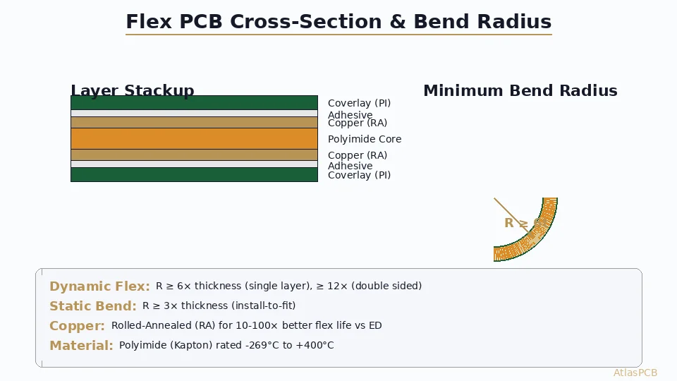
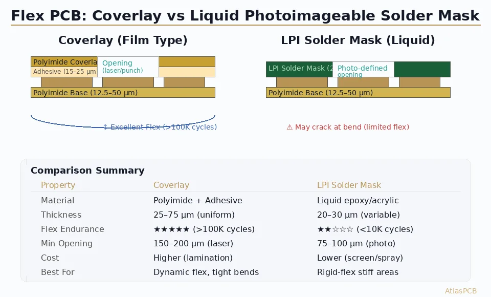
Polyimide cover film (12.5, 25, or 50 µm thickness): Provides chemical resistance, electrical insulation, and mechanical protection. The same polyimide (Kapton or equivalent) used for the base substrate ensures matched CTE and adhesion.
Adhesive layer (15, 25, or 50 µm thickness): Typically acrylic or modified epoxy. Bonds the cover film to the copper surface under heat and pressure during lamination (170–190°C, 150–300 PSI, 60–90 minutes).
Total coverlay thickness ranges from 27.5 µm (thinnest) to 100 µm (thickest standard option). Common configurations:
| Cover Film | Adhesive | Total | Application |
|---|---|---|---|
| 12.5 µm | 15 µm | 27.5 µm | Tight bend, thin flex |
| 25 µm | 25 µm | 50 µm | Standard dynamic flex |
| 25 µm | 50 µm | 75 µm | Filling over thick copper |
| 50 µm | 25 µm | 75 µm | High abrasion, connectors |
LPI Solder Mask for Flex
Flex-grade LPI solder mask uses modified formulations with increased flexibility compared to rigid-board mask. Key characteristics:
- Thickness: 15–30 µm (screen print) or 8–15 µm (spray coat)
- Flexibility: Can endure 5,000–10,000 bend cycles at 10 mm radius
- Resolution: 75–100 µm line/space, 75 µm minimum opening
- Application: Screen print, curtain coat, or inkjet
- Cure: UV exposure + thermal cure (150°C, 60 min)
Flex-specific LPI brands include Taiyo PSR-9000 FX series, Onstatic HF-series, and Peters SD 2467 FLX.
Head-to-Head Comparison
Mechanical Performance
Bend endurance is the critical differentiator:
| Parameter | Coverlay | LPI Solder Mask |
|---|---|---|
| Dynamic bend cycles (R=5mm) | >100,000 | 5,000–10,000 |
| Dynamic bend cycles (R=2mm) | >50,000 | <1,000 (fails) |
| Minimum static bend radius | 0.5 mm | 3.0 mm |
| Elongation at break | 70–100% | 5–15% |
| Pencil hardness | 2H–3H | 4H–6H |
| Abrasion resistance | Moderate | Low |
The reason is fundamental: polyimide film has 70–100% elongation at break, meaning it can stretch significantly before failing. Cured LPI epoxy has only 5–15% elongation — it’s a brittle material that fractures under relatively small strains.
Electrical Properties
| Property | Coverlay (Polyimide) | LPI Solder Mask |
|---|---|---|
| Dielectric constant (1 GHz) | 3.2–3.5 | 3.5–4.2 |
| Dissipation factor (1 GHz) | 0.002–0.005 | 0.015–0.030 |
| Dielectric breakdown | 300+ V/µm | 100–150 V/µm |
| Surface resistance | >10¹³ Ω | >10¹² Ω |
| CTI (tracking index) | 600V+ | 400–600V |
For [high-frequency flex circuits]/blog/flex-pcb-design-guidelines/) carrying RF signals, coverlay’s lower Df (0.003 vs 0.020) significantly reduces signal loss — a critical factor for 5G antenna feed networks and automotive radar flex assemblies.
Opening (Pad Access) Precision
This is where LPI solder mask has a decisive advantage:
Coverlay openings are created by:
- Laser cutting: 150–200 µm minimum opening, ±50 µm positional accuracy
- Die punching: 300–500 µm minimum opening, ±100 µm accuracy
- CNC routing: 500+ µm openings only
Because coverlay is applied as a pre-cut film, the openings cannot achieve the precision of photolithography. Registration between the coverlay openings and the copper pads depends on alignment during lamination — typically ±75–100 µm.
LPI openings are photo-defined after coating:
- 75–100 µm minimum opening
- ±25 µm registration accuracy
- Can define solder mask dams as narrow as 75 µm
For fine-pitch components (0.4 mm BGA, 0.5 mm QFN), LPI is often the only viable option for the pad area — even if the rest of the flex circuit uses coverlay.
Cost Structure
| Factor | Coverlay | LPI Solder Mask |
|---|---|---|
| Material cost | Higher (PI film + adhesive) | Lower (liquid resin) |
| Tooling | Die punch: $500–2,000 | Phototool: $50–200 |
| Labor (lamination) | Manual layup + press cycle | Automated print/spray |
| Cycle time | 90–120 min (press cure) | 30–60 min (UV + bake) |
| NRE impact | High for prototypes | Low (digital imaging) |
| Volume economics | Competitive at >1K pcs | Lower at all volumes |
FLEX & RIGID-FLEX PCB MANUFACTURING
Expert Flex PCB Fabrication with Coverlay & LPI Options
AtlasPCB manufactures 1–8 layer flex and rigid-flex PCBs with precision coverlay lamination, laser-cut openings, and IPC-6013 Class 3 reliability — prototype to volume.
Get Flex PCB Quote →Design Rules for Coverlay
Opening Design
Minimum copper-to-opening clearance: The adhesive from the coverlay will flow (“squeeze out”) during lamination. Design pad openings 100–150 µm larger than the pad on each side to compensate for adhesive flow.
Opening shape: Coverlay openings should avoid sharp internal corners, which create stress concentrators. Use radii ≥0.25 mm on all internal corners. For rectangular pad openings, round the corners.
Bridge (dam) width: The minimum polyimide bridge between adjacent openings is 0.5 mm for die-punch and 0.3 mm for laser-cut. Below these limits, the coverlay film lacks structural integrity and may tear during handling.
Bend Zone Rules
In dynamic bend areas, coverlay design must follow strict rules to prevent delamination:
No openings in bend zones: The coverlay must be continuous (no pad access) throughout any area that experiences repeated bending.
Copper conductor orientation: Route traces perpendicular to the bend axis. Traces parallel to the bend axis experience compression on the inner radius and tension on the outer radius, accelerating fatigue.
Staggered conductor placement: In multi-layer flex, stagger conductors on adjacent layers rather than stacking them directly above each other. This distributes bending strain more evenly.
Adhesive selection: For dynamic flex requiring >50,000 cycles, use acrylic-based adhesive (higher elongation) rather than epoxy-based adhesive. Specify “dynamic flex grade” coverlay from your supplier.
Minimum bend radius calculation: Per IPC-2223, minimum bend radius for dynamic flex = 6 × total thickness. For a 150 µm total stackup (25 µm coverlay + 50 µm PI base + 18 µm Cu + 25 µm coverlay + margins), minimum bend radius = 0.9 mm.
Stiffener Integration
Where flex circuits connect to connectors or carry heavy components, stiffeners provide local rigidity:
- FR-4 stiffener: 0.2–1.6 mm thick, bonded with pressure-sensitive adhesive or thermally laminated
- Polyimide stiffener: 0.05–0.3 mm, for moderate stiffening without excessive thickness
- Stainless steel stiffener: 0.1–0.3 mm, for EMI shielding + mechanical support
The stiffener boundary should extend at least 1.0 mm beyond the last pad to prevent stress concentration at the transition from stiff to flexible regions.
Design Rules for LPI Solder Mask on Flex
Application Methods
Screen printing: Standard method for flex-grade LPI. Provides 20–30 µm thickness. Works best on flat flex panels before singulation. Screen print cannot coat already-bent flex reliably.
Spray coating: 8–15 µm thickness per pass. Better conformality over conductor topography. Preferred for double-sided flex where screen printing causes coverage issues over via holes.
Inkjet (digital): Emerging technology. No phototool required. Excellent for prototypes. Thickness control of ±5 µm. Currently limited to small production volumes due to throughput.
When to Use LPI on Flex
LPI solder mask is appropriate in the following flex PCB scenarios:
Rigid sections of rigid-flex boards: The stiff areas bonded to FR-4 prepreg never bend. LPI provides finer feature resolution at lower cost.
Static flex applications: Flex circuits that bend only during installation (e.g., connecting two rigid boards inside a laptop) and never move again during product life.
Fine-pitch pad areas: When 0.4 mm pitch BGA or 0.5 mm CSP components are placed on a flex circuit, LPI may be required for the component footprint area — with coverlay used everywhere else.
EMI shielding layers: Some designs use a conductive-filled LPI as a shielding layer on the outer surface of a flex cable.
Hybrid Approach: Coverlay + LPI on the Same Board
Modern rigid-flex designs commonly use both materials:
- Flex zones: Coverlay with laser-cut openings for any pads in bend areas
- Rigid zones: LPI solder mask over the FR-4-bonded rigid sections
- Transition zones: Coverlay extends 2–3 mm past the rigid-flex boundary into the rigid area, overlapping with LPI by 1–2 mm for reliability
This hybrid approach requires careful manufacturing planning. The typical process sequence:
- Image and etch copper on flex layers
- Laminate coverlay over flex zones (heat + pressure)
- Bond flex to rigid layers with no-flow prepreg
- Drill through-holes through rigid sections
- Plate through-holes
- Apply and image LPI solder mask on rigid sections
- Surface finish (ENIG, ENEPIG, etc.)
IPC-6013 Requirements
For Class 3 reliability (military/aerospace/medical):
- Coverlay adhesion: ≥1.0 N/mm peel strength after thermal stress (6× solder float @ 288°C)
- No delamination after 500 thermal cycles (-65°C to +125°C)
- LPI adhesion (where used): ≥0.8 N/mm, no cracking after 3× reflow
Selecting the Right Material: Decision Framework
Use this decision tree:
Does the area bend during product life?
- Yes, >1000 cycles → Coverlay (mandatory)
- Yes, <1000 cycles → Coverlay recommended, LPI possible
- No (install-and-forget or rigid area) → Either material works
Are there fine-pitch pads (<0.5 mm pitch) in the area?
- Yes → LPI for pad area, coverlay for surrounding flex
- No → Coverlay can handle all openings
Frequency >3 GHz on flex traces?
- Yes → Coverlay (lower Df = less loss)
- No → Either material acceptable
Is cost the primary driver and bend endurance isn’t critical?
- Yes → LPI solder mask
- No → Coverlay for reliability margin
Failure Modes and Troubleshooting
Coverlay Failures
Delamination at openings: The most common coverlay failure. Caused by insufficient lamination pressure, contaminated copper surface (oxide, fingerprints), or opening design with sharp corners that create peel initiation points. Prevention: verify surface cleanliness with contact angle measurement (<30°), round all internal opening corners ≥0.25 mm radius.
Adhesive squeeze-out blocking pads: During lamination, the adhesive flows and can encroach into pad openings. If openings aren’t oversized by adequate margin (100–150 µm per side), adhesive covers solderable areas. Prevention: use thermography during lamination to verify adhesive flow behavior; adjust opening oversizing based on actual adhesive flow measurements for your specific coverlay.
Coverlay cracking at fold point: Occurs when bend radius is tighter than rated, or when coverlay is applied with excessive tension during layup. The crack propagates along the polyimide grain direction. Prevention: verify minimum bend radius calculation includes ALL layers (copper + base PI + coverlay + stiffeners); increase PI film thickness if operating near the limit.
LPI Solder Mask Failures on Flex
Cracking during bending: The #1 failure mode for LPI on flex. Brittle epoxy fractures when strain exceeds 2–3%. Always visible under 10× magnification as hairline cracks parallel to the bend axis. Prevention: never use standard LPI on dynamic flex areas; use flex-grade LPI formulations only for static areas.
Poor adhesion after thermal cycling: LPI on polyimide substrate has lower adhesion than on FR-4 due to the smooth PI surface. After 200+ thermal cycles (-40 to +125°C), CTE mismatch can cause delamination at the LPI/PI interface. Prevention: plasma-treat the PI surface before LPI application; use PI-compatible primer systems.
Undercut at openings: Photo-defined openings in flex-grade LPI can exhibit scalloped edges due to the modified (softer) formulation. This is cosmetic unless it exposes copper at pad edges. Prevention: increase mask-to-pad clearance by 25 µm compared to rigid-board rules.
Testing and Qualification
IPC-6013 Qualification Tests for Coverlay
For new coverlay materials or process qualification:
- Peel strength test: 25 mm strip, 90° peel at 50 mm/min. Pass: ≥1.0 N/mm for Class 3.
- Solder float test: 288°C for 10 seconds, 6 cycles. No delamination or blistering.
- Thermal cycling: -65°C to +125°C, 500 cycles. No cracking or delamination.
- Bend endurance: Specified bend radius and cycle count per design requirement.
- Chemical resistance: Flux, cleaning solvents, conformal coating. No degradation.
Production Verification
Every production lot should include:
- Cross-section analysis of coverlay adhesion and thickness uniformity
- Peel strength coupon test (destructive, 1 per panel or lot)
- Visual inspection for adhesive squeeze-out, bubbles, wrinkles
- Bend test sample (one flex circuit per lot bent to specification)
Manufacturing Partner Selection
When sourcing flex PCBs with coverlay, verify your manufacturer has:
- Hydraulic press or vacuum laminator rated for coverlay cure (170–190°C, 200+ PSI)
- Laser cutting system for coverlay openings (CO₂ or UV laser)
- Registration alignment accuracy ≤75 µm between coverlay and copper pattern
- [IPC-6013 Class 2 or 3 certification]/blog/ipc-6013-flexible-circuit-quality-standard/)
- Experience with your required bend radius and cycle count
Further Reading
- [Flex PCB Design Guidelines]/blog/flex-pcb-design-guidelines/)
- [Dynamic Flex PCB Design: Bend Radius & Reliability]/blog/dynamic-flex-pcb-design-bend-radius-reliability/)
- [IPC-6013 Flexible Circuit Quality Standard]/blog/ipc-6013-flexible-circuit-quality-standard/)
- [Rigid-Flex PCB Design: Bend Radius & Reliability Guide]/blog/rigid-flex-pcb-design-bend-radius-reliability-guide/)
- [PCB Solder Mask Application: LPI vs Dry Film vs Inkjet]/blog/pcb-solder-mask-application-lpi-vs-dry-film-inkjet/)
Building a flex or rigid-flex product? AtlasPCB’s engineering team reviews coverlay specifications, bend radius calculations, and hybrid stack-up designs before fabrication — ensuring first-pass reliability. Get a quote or view our flex PCB capabilities.
About AtlasPCB — We specialize in complex PCB manufacturing for HDI, RF, and high-reliability applications. Explore our rigid-flex PCB manufacturing, or get an full PCB manufacturing capabilities . Every order includes free engineering review. Get your quote.
Reviewed by AtlasPCB Engineering Team — IPC-certified manufacturing specialists with 15+ years of production experience in HDI, RF, and high-reliability PCB fabrication. Content based on factory floor data and real customer design reviews.
- flex pcb
- coverlay
- solder mask
- rigid-flex
- polyimide
- ipc-6013
- bend reliability