· AtlasPCB Engineering · Engineering · 6 min read
PCB DFM Check Before Ordering: 12-Point Verification That Prevents Costly Respins
A practical DFM verification checklist for engineers about to place a PCB fabrication order. Covers the 12 most common manufacturability issues that cause order rejection, yield loss, or design respins — with specific thresholds and how to fix each one.
Why DFM Matters More Than You Think
The cost of a DFM error is not the $50-150 NRE to fix a Gerber file. It is the 1-3 week delay for a respin, the $5,000-20,000 in engineering time to redesign, resimulate, and regenerate manufacturing files, and the project schedule impact when your boards arrive 4 weeks late.
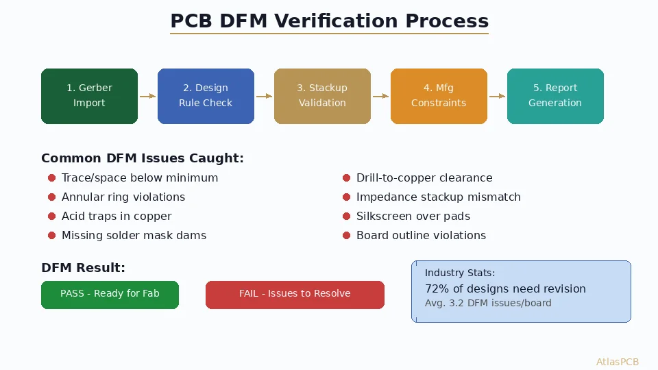
We review approximately 200 PCB designs per month before fabrication. Over 60% have at least one DFM issue that would cause order rejection or yield reduction. Here are the 12 most common problems, ranked by frequency of occurrence.
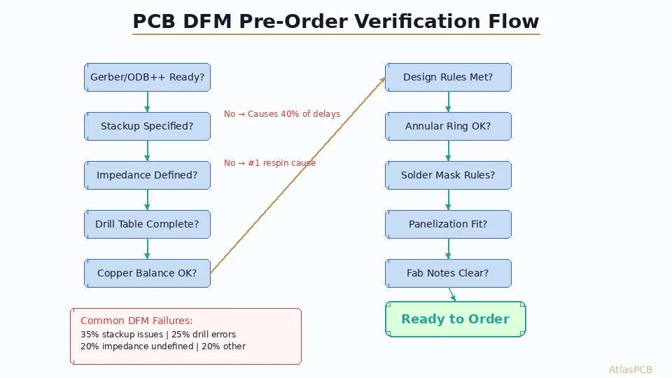
The 12-Point Pre-Order DFM Checklist
1. Minimum Trace Width and Space (Failure rate: 45%)
The problem: Designers route at theoretical minimums without margin for manufacturing variation.
The check: Your minimum trace/space must be ≥ your fabricator’s stated capability + 1mil margin for reliable yield.
| Fabricator Class | Stated Minimum | Design Target (with margin) |
|---|---|---|
| Budget (pooled panel) | 5/5 mil | 6/6 mil |
| Standard | 4/4 mil | 5/5 mil |
| Advanced (HDI) | 3/3 mil | 3.5/3.5 mil |
| Fine-line (mSAP) | 1.5/1.5 mil | 2/2 mil |
How to fix: Run minimum-width DRC at the target value (not the stated minimum). If violations exist, widen traces in non-critical areas or discuss with your fab partner whether their process can handle the specific geometry.
💡 Free DFM Check
Upload your Gerber files and our engineers will run a comprehensive DFM analysis within 24 hours — flagging not just violations but yield optimization opportunities. Submit for free DFM review →
2. Annular Ring Size (Failure rate: 38%)
The problem: The copper ring around drilled holes is too small after accounting for drill wander and layer registration tolerance.
The check: Minimum annular ring = (Pad diameter - Finished hole diameter) / 2 - Registration tolerance
For a 10-mil finished hole (12-mil drill before plating) in a 20-mil pad:
- Available annular ring: (20 - 12) / 2 = 4 mil
- Registration tolerance: +/-2 mil (standard), +/-1 mil (advanced)
- Effective annular ring: 4 - 2 = 2 mil ← VIOLATION (typical minimum is 3.5 mil)
Fix: Increase pad diameter to 24-26 mil, or use smaller drill size if hole size permits.
3. Drill-to-Copper Clearance (Failure rate: 32%)
The problem: Drilled holes pass too close to copper features on adjacent layers, risking short circuits after plating.
Minimum clearance: 8 mil from hole edge to nearest copper feature (for standard through-hole PCBs). HDI with laser vias: 5 mil minimum.
Where it hides: Via arrays near dense BGA breakout routing. Each via’s drill landing punches through inner layers where routing may be present.
4. Solder Mask Dam Width (Failure rate: 28%)
The problem: The strip of solder mask between adjacent pads is too narrow to survive the imaging and development process.
Minimum solder mask dam: 3 mil (75μm) for LDI-processed mask, 4 mil (100μm) for standard film. Below this, the dam washes away during development, creating solder bridges between pads during assembly.
Most common violator: 0.4mm-pitch BGA pads with NSMD (non-solder mask defined) openings. At 0.4mm pitch with 0.25mm pad, the mask opening leaves only 2.5-mil dam between adjacent openings.
5. Acid Trap Geometry (Failure rate: 22%)
The problem: Acute-angle trace junctions (below 90°) trap etchant during processing, causing over-etching or open circuits.
The check: All trace-to-trace and trace-to-pad junctions must form angles ≥ 90°. Most EDA tools flag this automatically, but custom copper pours and ground plane cutouts often create acid traps missed by standard DRC.
6. Copper Balance Across Layers (Failure rate: 20%)
The problem: Significant copper density difference between board sides causes warpage during lamination cooling.
The check: Compare copper fill percentage between top/bottom and between symmetric layer pairs. Difference > 20% between symmetric layers warrants adding copper fill (thieving) to the sparse layer.
7. Board Outline to Copper Clearance (Failure rate: 18%)
The problem: Copper features too close to the board edge get exposed or damaged during routing/scoring.
Minimum clearance: 10 mil (0.25mm) from board edge to any copper feature. For V-score separation: 15 mil minimum.
8. Via Aspect Ratio (Failure rate: 15%)
The problem: The ratio of board thickness to drill diameter exceeds plating capability, resulting in void formation in via barrels.
Maximum aspect ratio:
- Standard process: 8:1 (1.6mm board / 8mil drill = 10:1 → TOO HIGH)
- Advanced process: 10:1
- HDI microvia (laser): 1:1 maximum (depth = diameter)
9. Silkscreen Over Pad Violations (Failure rate: 12%)
The problem: Silkscreen (legend) overlapping SMD pads causes solder adhesion failures during assembly.
The check: Minimum 3-mil clearance from silkscreen to any exposed copper pad. Most EDA tools enforce this, but manual text additions and company logos frequently violate it.
10. Thermal Relief Connectivity (Failure rate: 10%)
The problem: Pads connected to large copper planes without thermal reliefs cannot be soldered reliably (heat sinks into the plane). Conversely, high-current pads that NEED solid connections are sometimes given thermal reliefs by default.
11. Panel Break-Tab Placement (Failure rate: 8%)
The problem: V-score or tab-routed panel separations that interfere with components or critical traces near the board edge.
12. Impedance Stackup Feasibility (Failure rate: 8%)
The problem: The specified impedance target is impossible with the chosen stackup and available materials.
Example: Requesting 50Ω on a 3-mil trace over a 4-mil dielectric with Dk 4.2 yields approximately 64Ω. The fabricator cannot adjust Dk — they can only adjust trace width or dielectric thickness. If neither is acceptable, the impedance target is unfeasible.
🔍 Avoid All 12 Issues — Let Us Check
Our engineering team runs full DFM analysis on every order before fabrication starts. We catch issues that automated tools miss and suggest optimization opportunities. Zero extra charge for standard DFM review. See our engineering review process →
Quick Self-Check Process
Before submitting your order:
- Run DRC with fabricator-specific rules (not your EDA default)
- Export Gerber files and reimport into a viewer (catches export errors)
- Check minimum features on each layer against fabricator capability table
- Verify drill table matches your layer stack (blind/buried via layer pairs)
- Open your fab drawing and confirm it matches the actual design intent
When to Accept DFM Compromises
Not every DFM warning requires a fix. Sometimes the design constraint is non-negotiable:
- 0.4mm pitch BGA requires tight mask dams → specify LDI solder mask
- High-density routing requires 3/3mil trace → specify HDI fabrication class
- Controlled impedance requires non-standard stackup → pay material premium
The key is knowing which compromises increase cost versus which cause rejection. Talk to your fabricator before finalizing — a 5-minute conversation can prevent a 5-week delay.
📨 Ready to Order? Get DFM-Verified Fabrication
AtlasPCB provides engineering-reviewed fabrication with proactive DFM feedback. We identify and resolve manufacturability issues before your boards hit the production line — no surprise rejections or yield problems. Upload Gerber for instant quote + DFM →
Related Reading
About AtlasPCB — We specialize in complex PCB manufacturing for HDI, RF, and high-reliability applications. Explore our free engineering DFM review . Every order includes free engineering review. Get your quote.
Reviewed by AtlasPCB Engineering Team — IPC-certified manufacturing specialists with 15+ years of production experience in HDI, RF, and high-reliability PCB fabrication. Content based on factory floor data and real customer design reviews.
- PCB DFM check
- DFM verification
- PCB ordering
- PCB fabrication
- design for manufacturing
- Gerber check