· AtlasPCB Engineering · Engineering · 6 min read
What Is a PCB? The Complete Beginner's Guide to Printed Circuit Boards
Learn the fundamentals of printed circuit boards (PCBs) - what they are, how they work, their basic structure, types, and applications across industries.

Printed Circuit Boards (PCBs) are the backbone of modern electronics. From the smartphone in your pocket to the control systems in commercial aircraft, virtually every electronic device relies on at least one PCB. But what exactly is a PCB, and why has it become so indispensable?
What Is a PCB?
A Printed Circuit Board (PCB) is a flat board made of insulating material with conductive pathways etched or printed onto its surface. These pathways — called traces — connect electronic components such as resistors, capacitors, integrated circuits (ICs), and connectors, enabling them to function as a complete circuit.
Before PCBs existed, circuits were built using point-to-point wiring. This method was error-prone, bulky, and nearly impossible to mass-produce. The invention of the PCB solved all these problems by providing a standardized, repeatable, and compact way to build electronic circuits.
A Brief History
- 1936: Paul Eisler, an Austrian engineer, created the first PCB as part of a radio set while working in England.
- 1940s: The U.S. military adopted PCB technology for use in proximity fuses during World War II.
- 1950s: The “auto-assembly” process was developed, enabling mass production.
- 1960s: Through-hole technology became standard, allowing components with wire leads to be inserted through drilled holes.
- 1980s: Surface Mount Technology (SMT) emerged, enabling smaller components to be soldered directly onto the board surface.
- 2000s-present: HDI (High Density Interconnect), flex PCBs, and advanced multi-layer designs pushed miniaturization further, enabling wearables, 5G, and IoT devices.
Basic Structure of a PCB
A typical PCB consists of several layers, each serving a critical function:
1. Substrate (Base Material)
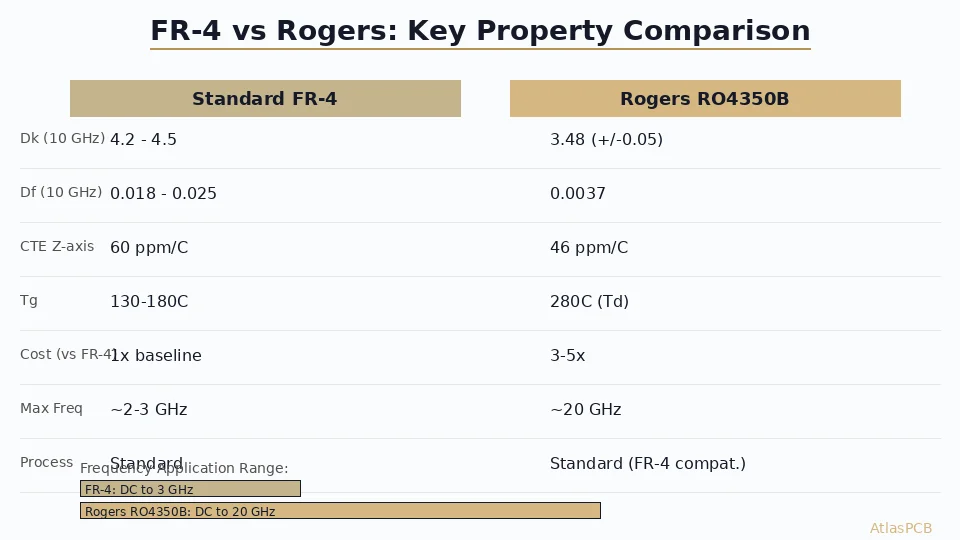
The foundation of the board. The most common substrate is FR-4, a glass-reinforced epoxy laminate. FR-4 offers good mechanical strength, electrical insulation, and heat resistance. For high-frequency applications, materials like PTFE (Teflon) or Rogers laminates are used.
- FR-4 Tg (glass transition temperature): 130-180 C
- FR-4 Dk (dielectric constant): 4.2-4.8 at 1 MHz
2. Copper Layer
Thin sheets of copper foil are laminated onto the substrate. The copper is then etched to form the circuit traces. Common copper weights include:
- 0.5 oz/ft2 (17 um): Fine-pitch, low-current applications
- 1 oz/ft2 (35 um): Standard for most designs
- 2 oz/ft2 (70 um): Power circuits requiring higher current
3. Solder Mask
A protective polymer layer (usually green, but also available in red, blue, black, white, and yellow) applied over the copper traces. It prevents accidental solder bridges during assembly and protects copper from oxidation and environmental damage.
4. Silkscreen
A printed layer of text and symbols on top of the solder mask. It labels components (R1, C5, U3), test points, logos, and polarity markings — essential for assembly and debugging.

Types of PCBs
By Layer Count
| Type | Layers | Typical Use |
|---|---|---|
| Single-sided | 1 copper layer | Simple consumer electronics, LED lighting |
| Double-sided | 2 copper layers | Most general electronics, IoT devices |
| Multi-layer | 4-30+ layers | Smartphones, servers, medical devices, aerospace |
By Rigidity
- Rigid PCB: Standard FR-4 boards that do not bend. Used in the vast majority of electronics.
- Flexible PCB: Made with polyimide film (e.g., Kapton), these boards can bend and fold. Common in wearables, cameras, and cable replacements.
- Rigid-Flex PCB: Combines rigid and flexible sections in a single board. Used in military, medical, and aerospace where space and reliability are critical.
By Special Construction
- Aluminum / Metal Core PCB (MCPCB): Uses an aluminum base for superior heat dissipation. Common in high-power LED lighting and automotive electronics.
- HDI PCB: Features microvias, fine traces, and high component density. Essential for smartphones, tablets, and advanced computing.
- High-Frequency PCB: Uses low-loss dielectric materials (PTFE, Rogers) for RF, microwave, and 5G applications.
How Do PCBs Work?
The working principle is straightforward:
- Conductive traces (copper pathways) route electrical signals and power between components.
- Vias (plated holes) connect traces on different layers of a multi-layer board.
- Pads provide soldering points where components are attached.
- The substrate provides mechanical support and electrical insulation between traces.
When power is applied, current flows through the copper traces following the designed circuit paths, enabling each component to perform its function — whether amplifying a signal, storing data, or controlling a motor.
Where Are PCBs Used?
PCBs are found in virtually every electronic device:
- Consumer Electronics: Smartphones, laptops, TVs, gaming consoles
- Automotive: Engine control units (ECU), infotainment systems, ADAS sensors
- Medical: MRI machines, pacemakers, patient monitors, diagnostic equipment
- Industrial: PLCs, motor drives, power supplies, robotics
- Telecommunications: 5G base stations, routers, switches, fiber optic transceivers
- Aerospace & Military: Avionics, satellite systems, radar, guidance systems
- IoT: Smart home devices, wearable sensors, environmental monitors
Key PCB Specifications to Know
When ordering a PCB, these are the critical parameters:
| Parameter | Common Values |
|---|---|
| Board thickness | 0.4mm, 0.8mm, 1.0mm, 1.2mm, 1.6mm (standard), 2.0mm |
| Copper weight | 0.5oz, 1oz, 2oz, 3oz |
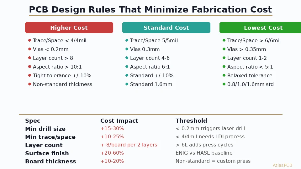
| Min trace width | 3mil (0.075mm) to 6mil (0.15mm) |
| Min trace spacing | 3mil to 6mil |
| Min drill size | 0.1mm (laser) to 0.3mm (mechanical) |
| Surface finish | HASL, ENIG, OSP, Immersion Silver |
| Solder mask color | Green, red, blue, black, white, yellow |
Why Choose Professional PCB Manufacturing?
While hobbyists can etch simple single-layer boards at home, professional manufacturing offers:
- Precision: Trace widths down to 3mil (0.075mm) with tight tolerances
- Reliability: Controlled impedance, consistent copper thickness, and rigorous testing
- Scalability: From prototype quantities (5-10 pieces) to mass production (100,000+)
- Quality Standards: IPC Class 2/3 compliance, UL certification, RoHS compliance
- Advanced Capabilities: Multi-layer stackups, blind/buried vias, HDI, flex circuits
Conclusion
PCBs are the unsung heroes of the electronics world. Understanding their basic structure, types, and applications is the first step toward better electronic product design. Whether you’re a student, hobbyist, or product engineer, knowing how PCBs work will help you make better decisions when designing, sourcing, and manufacturing electronic products.
At AtlasPCB, we specialize in providing high-quality PCB fabrication with fast turnaround times. Whether you need a simple 2-layer prototype or a complex 16-layer HDI board, our engineering team is here to help bring your designs to life.
Further Reading
[HDI PCB Design Guide: Stackup Rules, Via Structures & DFM Checklist]/blog/hdi-pcb-design-guide/)
[HDI PCB Technology: Microvias, Laser Drilling, and High-Density Design]/blog/hdi-pcb-technology/)
[Controlled Impedance PCB: Design, Stackup & Testing Explained]/blog/controlled-impedance-pcb/)
[Rogers 4350B vs FR4: When to Upgrade Your PCB Material]/blog/rogers-4350b-vs-fr4/)
[High-Frequency Microwave PCB Substrate Selection: Dk & Df Comparison of PTFE, Ceramic-Filled, and FR-4]/blog/high-frequency-pcb-substrate-selection-dk-df/)
[ENEPIG vs ENIG: Which PCB Surface Finish for Your Design?]/blog/enepig-vs-enig/)
[PCB Surface Finish Guide: HASL, ENIG, OSP and More Compared]/blog/pcb-surface-finish-guide/)
[PCB Solder Mask: Types, Colors, and Functions Explained]/blog/pcb-solder-mask-guide/)
[IPC Class 3 Requirements: The Complete Guide for Designers]/blog/ipc-class-3-requirements/)
[Rigid-Flex PCB Design: Stackup, Bend Rules, and Manufacturing Guidelines]/blog/rigid-flex-pcb-design/)
About AtlasPCB — We specialize in complex PCB manufacturing for HDI, RF, and high-reliability applications. Explore our full PCB manufacturing capabilities, or get an instant online quote . Every order includes free engineering review. Get your quote.
Reviewed by AtlasPCB Engineering Team — IPC-certified manufacturing specialists with 15+ years of production experience in HDI, RF, and high-reliability PCB fabrication. Content based on factory floor data and real customer design reviews.
- pcb basics
- beginner guide
- electronics