· AtlasPCB Engineering · Engineering · 7 min read
PCB Panelization and Depaneling: V-Score, Tab Routing, and Laser Singulation Methods
Master PCB panelization design with v-scoring, tab routing, and laser depaneling. Learn panel array optimization, breakaway tab design rules, stress-free singulation for sensitive assemblies, and cost-per-unit panel efficiency calculations.
Why Panelization Matters
A single PCB unit rarely goes through SMT assembly alone. Pick-and-place machines, reflow ovens, wave soldering systems, and AOI stations are all designed to handle standard panel sizes — typically 250×330 mm, 250×460 mm, or custom sizes per the assembler’s rail specifications.
Panelization determines:
- Assembly cost — More units per panel = lower cost per unit
- Component quality — Improper depaneling stresses components
- Edge quality — Connector fit and EMI performance depend on clean edges
- Yield — Poor panel utilization wastes substrate material
Panel Design Fundamentals
Standard Panel Sizes
| Region | Common Panel Size | Usable Area | Tooling Rails |
|---|---|---|---|
| Asia (China) | 250 × 330 mm | 230 × 310 mm | 10 mm each side |
| Asia (large) | 250 × 460 mm | 230 × 440 mm | 10 mm each side |
| Europe/US | 229 × 305 mm (9×12”) | 209 × 285 mm | 10 mm each side |
| Custom | Per assembler spec | Varies | 5-15 mm |
Tooling Rail Requirements
Tooling rails (also called breakaway edges or panel borders) provide:
- Fiducial marks for machine alignment (minimum 2, preferably 3)
- Conveyor rail support edges (minimum 5 mm flat edge)
- Tooling holes (3× ø3.2 mm or 2× ø4.0 mm holes, positioned symmetrically)
- Bad-mark areas for selective assembly of known-good units
- Text markings: panel barcode, date code, fabricator info
Array Optimization
Maximizing units per panel directly reduces cost:
Units per panel = floor(Usable_X / (Unit_X + Gap)) × floor(Usable_Y / (Unit_Y + Gap))Where Gap = minimum routing channel width (typically 2.0-2.5 mm for tab routing, 0 mm for v-score).
Example: 30×40 mm boards on a 230×310 mm usable area:
- Portrait: floor(230/32) × floor(310/42) = 7 × 7 = 49 units
- Landscape: floor(230/42) × floor(310/32) = 5 × 9 = 45 units
- Rotated 90° mix: try both orientations and pick the best
Pro tip: Also try a 2-up rotation where alternating rows are flipped 180°. This can improve utilization for non-rectangular or odd-shaped boards.
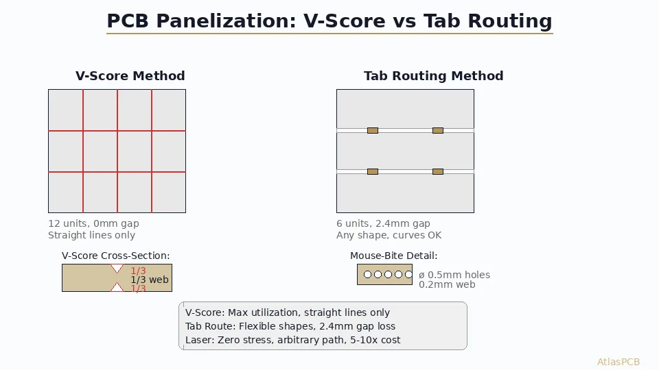
V-Score (V-Groove) Depaneling
How V-Scoring Works
A v-shaped blade scores parallel grooves on the top and bottom of the panel. Each groove penetrates approximately 1/3 of the board thickness, leaving the center 1/3 as the breakaway web.
Cross-section:
  Top surface:      \  /  ← 30° included angle
                     \/   ← 1/3 depth
  Remaining web:    ====  ← 1/3 thickness
  Bottom groove:    /\    ← 1/3 depth
                   /  \   ← 30° included angle
  Bottom surface:
V-Score Design Rules
| Parameter | Typical Value | Range |
|---|---|---|
| Groove angle | 30° | 20°-60° |
| Residual web | 0.3-0.5 mm | Min 0.2 mm |
| Score accuracy | ±0.1 mm | Position to board edge |
| Board thickness | 0.8-3.2 mm | Outside this: tab routing preferred |
| Component keep-out | 1.0 mm minimum | 2-3 mm for sensitive |
V-Score Advantages
- Zero routing gap — Boards sit edge-to-edge, maximizing panel utilization
- Fast processing — One pass per score line, regardless of panel length
- Low cost — Simple tooling, fast cycle time
- Strength during assembly — Full-width connection supports heavy components
V-Score Limitations
- Straight lines only — Cannot score curves or notches
- Full-panel lines — Score must run edge-to-edge; cannot start/stop mid-panel
- Edge roughness — Fractured surface is uneven (±0.1 mm)
- Board stress — Breaking generates bending moment that can crack nearby components
- Thickness dependent — Too thin (<0.6 mm) may break during assembly; too thick (>3.2 mm) is hard to break
Depaneling Methods for V-Score
- Manual break: Operator bends along score line — uncontrolled stress, not recommended for production
- Pizza cutter: Rotary blade runs along the score — moderate stress, fast
- Guillotine: Linear blade shears the web — clean cut, some lateral stress
- Automated depaneling machine: Controlled break with board supported on both sides — lowest stress
Tab Routing (Breakaway Tabs with Mouse-Bites)
Need Panelization Design Review?
AtlasPCB's engineers optimize your panel layout for maximum yield and stress-free depaneling. Free DFM review included with every order.
Submit Your Design →How Tab Routing Works
A CNC router cuts the board outline with a 2.0 mm end mill, leaving small uncut sections (tabs) that hold the board in the panel. Each tab contains a row of drilled holes (mouse-bites) that create a perforated line for easy breakout.
Tab Design Parameters
| Parameter | Standard | High-Reliability |
|---|---|---|
| Tab width | 3-5 mm | 5-8 mm |
| Tab thickness | Full board thickness | Full |
| Mouse-bite hole ø | 0.5-0.8 mm | 0.5 mm |
| Holes per tab | 3-5 | 5-7 |
| Web between holes | 0.2-0.3 mm | 0.15-0.25 mm |
| Number of tabs | 3-5 per board | 4-6 per board |
| Max tab spacing | 75 mm | 50 mm |
Tab Placement Strategy
- Place tabs at corners for maximum panel rigidity
- Avoid placing tabs near sensitive components (BGA, crystal, sensors)
- For rectangular boards: 2 tabs per short edge, 1-2 per long edge
- For irregular shapes: minimum 3 tabs with ≥120° angular spread
- Never place a tab mid-way along a flex zone or controlled-impedance edge
Routed Slot Dimensions
- Minimum routing gap: 2.0 mm (for 2.0 mm end mill)
- Preferred routing gap: 2.4 mm (allows tool wear before undersizing)
- Corner radius: matches end mill diameter (1.0 mm radius for 2.0 mm tool)
- For internal cutouts: minimum 2.0 mm tool access from panel edge
Mouse-Bite Breakout Quality
After breaking tabs, small nubs remain on the board edge:
- Nub height: 0.1-0.3 mm typical
- Can be sanded/filed for clean edge (manual labor, additional cost)
- Automated deflashing available for high volume
- For enclosure-critical edges, use v-score on that edge instead
Laser Singulation
Process Overview
UV or CO₂ laser ablates the board material along the programmed cut path. No mechanical force contacts the board.
Laser Parameters
| Type | Wavelength | Best For | Cut Speed |
|---|---|---|---|
| UV (Nd:YAG) | 355 nm | Thin boards (<1.0 mm), flex | 5-20 mm/s |
| CO₂ | 10.6 µm | Standard FR-4 (0.8-2.0 mm) | 10-50 mm/s |
| Green (Nd:YAG) | 532 nm | Medium thickness, mixed materials | 8-30 mm/s |
Laser Advantages
- Zero mechanical stress — No bending, no vibration, no component cracking
- Arbitrary cut paths — Curves, notches, tight corners possible
- Precision: ±0.05 mm edge position
- No dust/debris (UV laser with extraction)
- No tooling wear — Consistent cut quality over entire production run
Laser Limitations
- Carbonization — Laser heat creates conductive carbon residue on cut edges (must be cleaned for high-voltage applications)
- Speed — 5-10× slower than v-score per panel
- Cost — Equipment cost >$200K; processing cost 5-10× mechanical methods
- Thickness limit — Most practical up to 1.6 mm; thicker boards require multiple passes
- FR-4 challenges — Glass fiber scattering creates uneven cut edges on thick boards
When to Specify Laser Depaneling
- Flexible/rigid-flex circuits
- Boards with components within 0.5 mm of edge
- BGA or QFN near panel separation line
- Ceramic or brittle substrate materials
- Medical/aerospace with zero-tolerance for hidden stress damage
Panelization for Mixed PCB Designs
Multi-Up Panels (Different Designs)
Combining different PCB designs on one panel can save cost for small production runs:
Rules:
- All designs must share: same layer count, same copper weight, same surface finish
- Tooling holes and fiducials on shared rails
- Clearly mark each design with unique identifier
- Separate depaneling may require different tab configurations
Risks:
- Different thermal mass → uneven reflow
- Different component heights → stencil/inspection complexity
- BOM management complexity at assembly
- Not recommended for production volumes >500 panels
Castellated Edge Panels
Module PCBs with castellated (half-hole) edges require special panel design:
- Route through the center of castellated pads
- Plated half-holes must be on the routed edge, not v-score
- Tab routing creates the half-circle automatically
- Additional plating step may be needed for exposed copper quality
Cost Impact Analysis
Panel Utilization vs. Cost
Cost per unit = (Panel cost × (1 + scrap_rate)) / Units_per_panelExample comparison for a 25×35 mm board:
| Method | Gap Loss | Units/Panel | Relative Cost |
|---|---|---|---|
| V-score (both axes) | 0 mm | 63 units | 1.00× (baseline) |
| Tab routing | 2.4 mm | 49 units | 1.28× |
| V-score X + tab Y | 0/2.4 mm | 56 units | 1.13× |
The 28% cost increase from tab routing buys you:
- Ability to handle irregular board shapes
- Reduced component stress during depaneling
- Better edge quality for enclosure fit
Volume Thresholds for Method Selection
| Volume | Recommended Method | Reason |
|---|---|---|
| Prototype (<50) | Tab routing | Flexibility, low NRE |
| Low volume (50-5K) | V-score or tab | Cost optimize per geometry |
| Medium (5K-100K) | V-score preferred | Fastest, cheapest per unit |
| High (>100K) | V-score + auto depanel | Throughput critical |
| Sensitive assemblies | Laser or router depanel | Quality over cost |
Quality Defects and Prevention
Solder Joint Cracking During Depaneling
Root cause: Bending stress during v-score break transfers to BGA/QFN joints. Prevention:
- Increase keep-out to 3 mm for BGA
- Use controlled-break depaneling fixture
- Switch to tab routing for boards with BGA near edges
Board Warpage Post-Depaneling
Root cause: Residual stress from asymmetric copper distribution released when panel constraint removed. Prevention:
- Balance copper on all layers
- Include copper thieving in border areas
- Allow stress-relief cuts (score or slot) between asymmetric zones
Micro-Crack Formation
Root cause: Mechanical shock during manual break or high-speed router depaneling. Prevention:
- Reduce depaneling speed
- Support board on both sides during separation
- Post-process inspection with side-lighting for crack detection
Further Reading
- Copper Balancing and Thieving for PCB: Preventing Warpage
- BGA Pad Design: Via-in-Pad and Solder Voiding Prevention
- PCB Layer Registration and Alignment Tolerance
- DFM for Fine-Pitch BGA PCB Design
Need optimized panelization for your next production run? AtlasPCB engineers review every panel design for maximum utilization and minimum depaneling stress. Our standard DFM check includes panelization optimization at no extra charge. Get a quote or explore our manufacturing capabilities.
About AtlasPCB — We specialize in complex PCB manufacturing for HDI, RF, and high-reliability applications. Explore our PCB assembly services . Every order includes free engineering review. Get your quote.
Reviewed by AtlasPCB Engineering Team — IPC-certified manufacturing specialists with 15+ years of production experience in HDI, RF, and high-reliability PCB fabrication. Content based on factory floor data and real customer design reviews.
- panelization
- depaneling
- v-score
- tab routing
- PCB assembly
- laser singulation
- panel array