· AtlasPCB Engineering · Engineering · 6 min read
PCB Land Pattern Design: IPC-7351B Footprint Standards for SMD Components
Master IPC-7351B land pattern design for SMD components. Learn density levels, pad dimension calculations, courtyard rules, and thermal relief for optimal PCB assembly yield.
Why Land Pattern Design Determines Assembly Yield
The land pattern — also called a footprint or pad pattern — is the copper geometry on a PCB that receives a surface-mount component’s leads or terminations. A correctly designed land pattern ensures:
- Reliable solder joint formation during reflow
- Self-centering of components through surface tension
- Adequate solder fillet size for inspection and reliability
- Sufficient clearance for rework tools
- Compliance with IPC-A-610 workmanship standards
An undersized pad reduces solder joint volume, leading to premature fatigue failures. An oversized pad wastes routing space and can cause bridging on fine-pitch components. IPC-7351B provides the engineering framework to calculate optimal dimensions for any SMD component.

IPC-7351B Fundamentals
Document Scope and History
IPC-7351B (“Generic Requirements for Surface Mount Design and Land Pattern Standard”) is the definitive industry standard for SMD land pattern calculations. It replaced the older IPC-SM-782 standard and provides:
- Mathematical formulas for calculating pad dimensions from component geometry
- Three density-level options for different assembly environments
- Courtyard definitions for component spacing
- Thermal management pad guidelines
- Via-in-pad considerations
The Three Density Levels
IPC-7351B defines three environment categories that determine pad size extensions:
Level M — Most (Maximum)
- Largest pads, most solder, easiest rework
- Environment: Low-density boards, prototype, hand-assembly
- Courtyard excess: 0.5mm per side
- Toe fillet extension: 0.55mm
Level N — Nominal (Standard)
- Balanced pads for automated production
- Environment: Standard production, reflow soldering
- Courtyard excess: 0.25mm per side
- Toe fillet extension: 0.35mm
Level L — Least (Minimum)
- Smallest pads, maximum routing density
- Environment: High-density, mobile, wearables
- Courtyard excess: 0.1mm per side
- Toe fillet extension: 0.15mm
Pad Dimension Calculation Method
Basic Formula
For a gull-wing lead (QFP, SOP, SSOP):
Pad Length (Z) = Lead Span Max + 2×(Toe Extension) + Tolerance
Pad Width (X) = Lead Width Max + 2×(Side Extension) + Tolerance

Where:
  Toe Extension (Jt) = solder fillet beyond lead toe
  Heel Extension (Jh) = solder fillet at heel
  Side Extension (Js) = solder fillet at sides
  Tolerance = √(component tolerance² + board tolerance² + placement tolerance²)
Extension Values by Component Type
| Component Family | Jt (toe) | Jh (heel) | Js (side) | Notes |
|---|---|---|---|---|
| Gull-wing (QFP) | 0.55/0.35/0.15 | 0.45/0.35/0.25 | 0.05/0.03/0.01 | M/N/L levels |
| J-lead (PLCC) | 0.55/0.35/0.15 | 0.10/0.00/-0.10 | 0.05/0.03/0.01 | Heel under body |
| Chip (0402-2512) | 0.55/0.35/0.15 | 0.00/-0.05/-0.10 | 0.05/0.03/0.01 | Two-terminal |
| BGA | N/A | N/A | N/A | Pad = ball diameter × 0.75-1.0 |
| QFN (exposed pad) | 0.55/0.35/0.15 | 0.00/0.00/0.00 | 0.05/0.03/0.01 | Plus thermal pad |
Worked Example: 0.5mm Pitch QFP-64
Component specifications:
- Lead pitch: 0.5mm
- Lead width: 0.22mm (max 0.27mm)
- Lead length: 0.6mm (max 0.75mm)
- Lead span: 11.75mm - 12.25mm
Nominal (Level N) calculation:
- Pad width = 0.27 + 2×0.03 + 0.05 = 0.38mm → round to 0.35mm
- Pad length = 0.75 + 0.35 + 0.35 + 0.05 = 1.50mm
- Pad center from origin = (12.00/2) + (1.50/2) - 0.75 = 5.25mm
The resulting pad is 0.35mm × 1.50mm centered at 5.25mm from package center.
Courtyard Design Rules
Purpose of the Courtyard
The courtyard defines the minimum area that must remain free around each component. It accounts for:
- Component body overhang
- Lead protrusion beyond body
- Land pattern extent beyond leads
- Assembly tolerance
- Pick-and-place nozzle clearance
- Rework tool access
Courtyard Calculation
Courtyard boundary = Component maximum body dimension
                   + Lead extent beyond body
                   + Courtyard excess (per density level)

Round outward to nearest 0.05mm grid
Let Us Review Your Footprint Library Before Production
AtlasPCB's DFM team validates land patterns against IPC-7351B and our process capabilities. Catch pad errors before they become assembly defects.
Request DFM Review →Courtyard Overlap Rules
When component courtyards overlap:
- Same-side components: Minimum 0.25mm gap between courtyards (Level N)
- Opposing-side components: Courtyards may overlap if thermal profiles are compatible
- Tall components next to short: Consider shadow during wave soldering
Thermal Pad Design for QFN and Exposed-Pad Packages
Ground/Thermal Pad Sizing
QFN and similar packages have a large exposed pad on the bottom for thermal dissipation. IPC-7351B recommends:
- Pad size = 80-100% of exposed pad dimension
- Solder paste coverage: 50-80% of pad area (windowed stencil)
- Via array in thermal pad: minimum 4 vias per 5mm² area
- Via diameter: 0.3mm, plugged with epoxy to prevent solder wicking
Stencil Aperture Design for Thermal Pads
A single large stencil aperture over the thermal pad causes voiding. Best practice:
Aperture design for thermal pad:
- Divide into grid of smaller openings (1.0×1.0mm typical)
- Gap between openings: 0.3-0.5mm
- Total paste area: 50-60% of pad area
- Paste height: 0.125-0.150mm (5-6mil)
This window-pane pattern allows flux gases to escape, reducing void area to < 25% per IPC-7093.
Special Cases and Advanced Topics
0201 and 01005 Components
Ultra-miniature chip components require special attention:
0201 (0.6×0.3mm):
- Pad size: 0.35×0.30mm (Level N)
- Pad gap: 0.20mm
- Solder paste: Type 5 or Type 6
- Stencil thickness: 0.075-0.100mm
01005 (0.4×0.2mm):
- Pad size: 0.25×0.20mm (Level L only)
- Pad gap: 0.15mm
- Solder paste: Type 6 or Type 7
- Requires laser-cut stencil with electroformed apertures
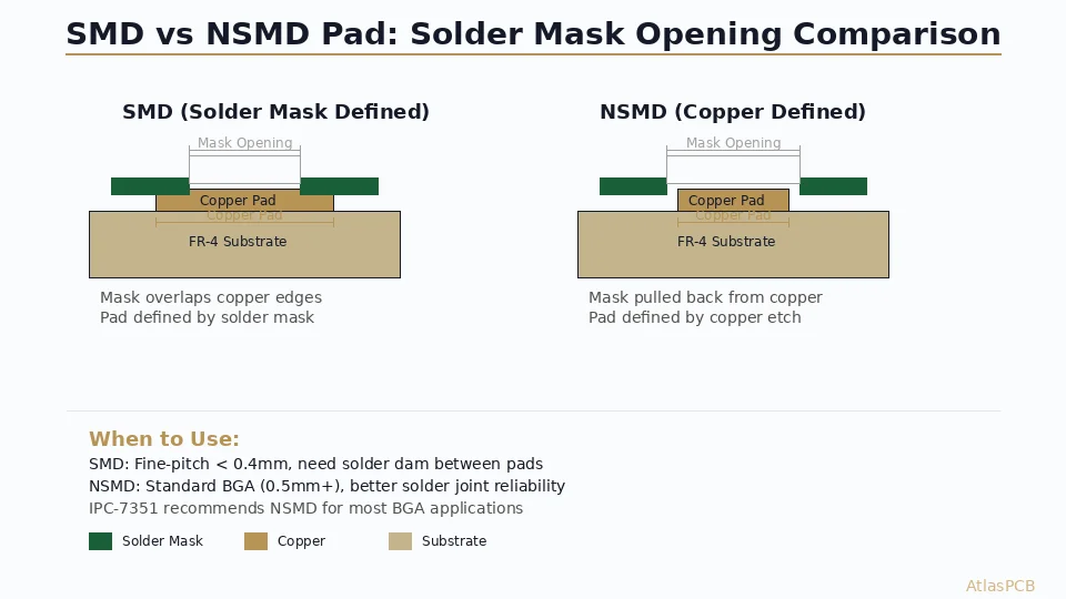
BGA Land Patterns
BGA pad calculation differs from leaded components:
Non-Solder Mask Defined (NSMD):
  Pad diameter = Ball diameter × 0.75 (for 0.5mm pitch)
  Pad diameter = Ball diameter × 0.80 (for 0.8mm+ pitch)
  Solder mask opening = Pad + 0.075mm per side

Solder Mask Defined (SMD):
  Pad diameter = Ball diameter × 1.0
  Solder mask opening = Ball diameter × 0.80
  Used when trace routing between pads is impossible
NSMD pads are preferred because they provide:
- Stronger solder joint (solder wraps around pad edge)
- Better thermal fatigue resistance
- More consistent ball collapse during reflow
Connector and Through-Hole Mixed Technology
For boards with both SMD and through-hole components:
- Through-hole pad annular ring: IPC-6012 minimum per class
- Wave solder side SMD pads: Add 0.1mm to all extensions
- Selective soldering pads: Standard IPC-7351B dimensions apply
- Thermal relief for ground plane connections: 4-spoke, 0.3mm spoke width
Library Naming Convention (IPC-7351B)
IPC-7351B defines a standard naming convention for land patterns:
Format: FAMILY_PINS_BODY-WIDTH_BODY-LENGTH_PITCH_DENSITY

Examples:
  SOIC127P600X175-8N  → SOIC, 1.27mm pitch, 6mm wide, 8 pins, Nominal
  QFP50P1200X1200X160-64N → QFP, 0.5mm pitch, 12×12mm body, 64 pins
  CHIP0805L → 0805 chip component, Least density
  BGA127P13X13_1400X1400X185-169N → BGA, 1.27mm pitch, 13×13 array
This systematic naming enables:
- Unambiguous communication between design and manufacturing
- Automated library management
- DFM rule checking against density level
Common Land Pattern Mistakes
1. Incorrect Component Orientation Mark
The pin-1 indicator must be placed within the courtyard. Ambiguous orientation leads to 180° placement errors — the most common SMT assembly defect.
2. Pad-to-Mask Registration Error
Solder mask registration tolerance is typically ±0.05mm. If pad-to-mask clearance is less than this tolerance, mask may partially cover the pad, causing solder rejection. Minimum solder mask clearance: 0.05mm per side (Level L) to 0.075mm (Level N).
3. Insufficient Pad-to-Pad Gap
Minimum copper-to-copper gap between pads must account for:
- Fabrication etching tolerance (±0.025mm for standard, ±0.015mm for HDI)
- Solder bridging risk (gap < 0.15mm requires solder dam)
- Electrical clearance per IPC-2221 (voltage dependent)
4. Missing Thermal Relief on Power Pads
Large ground/power pads connected to plane layers without thermal relief create a heat sink effect during soldering, causing cold joints. Always specify 4-spoke thermal relief with 0.25-0.30mm spoke width for wave and selective soldering.
Validating Your Land Patterns
Before releasing to fabrication, validate land patterns against:
- Component datasheet — Verify all dimensions match recommended footprint
- IPC-7351B calculator — Check mathematical compliance for chosen density level
- 3D model interference — Confirm component body doesn’t conflict with adjacent parts
- DFM check with fabricator — Verify against actual process capabilities
- Assembly trial — First-article inspection per IPC-A-610
Further Reading
- PCB Solder Paste and Stencil Design Guide
- DFM for Fine-Pitch BGA PCB Design Rules
- AOI and SPI Inspection for PCB Assembly Quality Control
- PCB Design Rules: Trace Width and Spacing
Need land pattern validation for your next production run? AtlasPCB’s DFM engineers review every design against IPC-7351B standards and our manufacturing process windows. Get your free DFM review →
About AtlasPCB — We specialize in complex PCB manufacturing for HDI, RF, and high-reliability applications. Explore our PCB assembly services, free engineering DFM review, or get an full PCB manufacturing capabilities . Every order includes free engineering review. Get your quote.
Reviewed by AtlasPCB Engineering Team — IPC-certified manufacturing specialists with 15+ years of production experience in HDI, RF, and high-reliability PCB fabrication. Content based on factory floor data and real customer design reviews.
- IPC-7351
- land pattern
- footprint design
- SMD
- PCB assembly
- DFM
- component library