· AtlasPCB Engineering · Engineering · 9 min read
Rogers 4350B PCB Stackup Design: Layer Configuration, Hybrid Builds, and Manufacturing Specs
Complete engineering guide to Rogers RO4350B stackup design. Covers 4-layer to 10-layer configurations, hybrid Rogers/FR-4 builds, prepreg selection, copper weight planning, and the manufacturing constraints that determine whether your stackup is actually producible.
Quick Reference: Rogers 4350B Material Properties
| Property | Value | Design Impact |
|---|---|---|
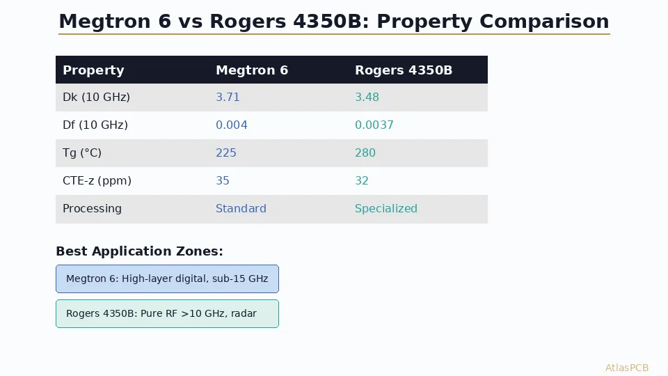
| Dk (10 GHz) | 3.48 ±0.05 | Enables tight impedance prediction |
| Df (10 GHz) | 0.0037 | 5x lower loss than standard FR-4 |
| CTE (X/Y) | 10-12 ppm/C | Compatible with FR-4 hybrid builds |
| CTE (Z) | 32 ppm/C | Lower via stress than FR-4 (Z: 60-70 ppm/C) |
| Tg | >280C (thermoset) | Survives multiple reflow cycles |
| Td | 390C | High decomposition temperature |
| Processing | Standard FR-4 equipment | No special tooling required |
| Core thicknesses | 6.6-60mil | Wide range for impedance targets |
The combination of low loss tangent, tight Dk tolerance, and FR-4-compatible processing makes RO4350B the default choice for RF PCBs operating between 2-20 GHz. Above 20 GHz (mmWave 5G, 77 GHz automotive radar), PTFE-based Rogers materials outperform, but below that frequency range, RO4350B delivers the optimal cost-performance balance.
Stackup Architecture: From 4-Layer to 10-Layer
4-Layer Hybrid: The Most Common RF Configuration
The 4-layer hybrid Rogers/FR-4 stackup handles approximately 60% of RF PCB applications we fabricate. The architecture is straightforward: RO4350B serves as the L1-L2 core carrying RF traces on L1 (microstrip) with an immediate ground plane reference on L2. Layers 3-4 use FR-4 for power distribution and low-speed digital routing.
In our production line, we typically build this as: L1 (1oz copper, RF traces) on RO4350B 10mil core, bonded with 4450F prepreg to L2 (ground plane), then FR-4 2116 prepreg bonding to L3 (power/digital), with FR-4 core to L4 (ground/digital). Total thickness lands between 1.0-1.6mm depending on copper weights and prepreg selection. The critical dimension is the L1-L2 dielectric thickness — this controls your microstrip impedance, and RO4350B’s ±0.5mil thickness tolerance (pressed) gives us the consistency needed for ±5% impedance control.
A common engineering mistake is placing the Rogers core between L2-L3 instead of L1-L2. This forces stripline topology for RF signals, which has 2x the conductor loss compared to microstrip because the signal is surrounded by dielectric on both sides. Unless you specifically need stripline for shielding reasons (automotive EMC compliance, for example), microstrip on L1 with RO4350B delivers better insertion loss.
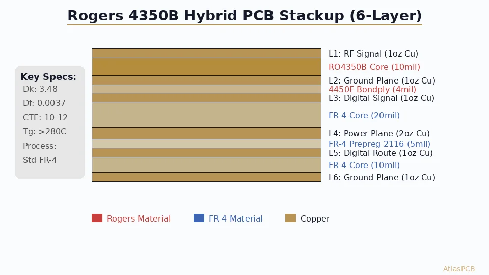
6-Layer Hybrid: Dual-Band and Mixed-Signal
When your design requires both RF performance and significant digital routing density — common in wireless modules combining WiFi/Bluetooth with a microcontroller — the 6-layer hybrid provides dedicated domains:
L1: RF traces (RO4350B core to L2) — antenna feeds, PA output, LNA input L2: Ground plane (continuous, unbroken under RF traces) L3: High-speed digital (FR-4 core to L4) — DDR, SPI, USB L4: Power plane / slow digital L5: Digital routing L6: Ground plane
The key design rule: maintain an unbroken ground plane on L2 directly beneath all RF traces on L1. Any slot, via antipad, or split in this ground plane creates a return path discontinuity that radiates and increases insertion loss. We see this mistake in roughly 20% of RF designs that come through our DFM review — and it typically costs 3-6 dB of performance that designers spend weeks debugging before discovering it is a layout problem.
STACKUP REVIEW SERVICE
Get Your Rogers Stackup Validated Before Fabrication
Upload your stackup design — our RF process engineers verify impedance targets, material compatibility, and manufacturability. Avoid costly respins from incorrect layer assignments.
Submit Stackup for Review ›8-10 Layer: Full RF System Integration
For complex RF systems — phased array modules, multi-band base station filters, or integrated RF/digital SoC carriers — 8-10 layer hybrid stackups provide complete isolation between RF, digital, and power domains. The architecture typically assigns 2-3 layers to Rogers-based RF signal pairs with dedicated ground planes, while the remaining layers handle high-speed digital interfaces (PCIe, DDR), power distribution networks, and slow control signals.
At 8+ layers with Rogers material, the stackup engineering becomes critical. Our process engineers typically recommend no more than 2-3 Rogers cores in the stack, positioned symmetrically to prevent warpage during lamination. An asymmetric Rogers placement — for example, RO4350B on L1-L2 only in a 10-layer build — creates a CTE imbalance that can cause 2-3mm/100mm bow and twist exceeding IPC-6012 Class 2 limits (0.75%).
The lamination sequence also matters: Rogers cores should be bonded in the first press cycle with their adjacent ground planes, then the full stack assembled in subsequent cycles. This ensures the Rogers/copper interface sees maximum bonding pressure and temperature, critical for long-term adhesion reliability in thermal cycling environments.
Manufacturing Constraints You Must Design For
Drill Compatibility
RO4350B machines identically to FR-4 — standard carbide drill bits, entry/backup materials, and hit counts apply. This is the material’s primary advantage over PTFE, which requires specialized drilling parameters to prevent smearing and delamination. In our facility, we process RO4350B with the same drill programs as FR-4 panels without parameter changes, achieving hole position accuracy within ±50μm and zero drill smear requiring desmear processing.
However, laser drilling for microvias on RO4350B requires adjusted parameters. The material ablates differently from FR-4 due to its ceramic filler content (proprietary woven glass + ceramic), requiring ~15% higher energy density and adjusted pulse counts. If your design requires HDI microvias on Rogers layers, confirm your manufacturer has characterized laser parameters specifically for RO4350B — not all shops have.
Copper Adhesion and Surface Preparation
RO4350B provides standard copper adhesion (peel strength >6 lb/in) suitable for all surface finish processes including ENIG, immersion silver, and OSP. No special surface preparation is required beyond standard oxide treatment for multilayer bonding. This contrasts with PTFE materials (RO3000 series) that require sodium etch or plasma treatment for adequate adhesion — adding cost and process complexity that RO4350B avoids entirely.
Solder Mask Considerations
Standard LPI (liquid photoimageable) solder mask adheres well to RO4350B surfaces. The one exception: if your design uses the Rogers material on outer layers with very fine-pitch features (0.15mm pad spacing or below), the slight surface texture difference from FR-4 can affect mask registration. Our recommendation is to use 75μm mask-defined openings rather than solder-mask-defined pads on Rogers outer layers to maintain adequate process margin.
CHINA RF PCB MANUFACTURER
Rogers 4350B Stackups — Fabricated Weekly
We maintain Rogers RO4350B and RO4003C inventory for fast turnaround. Hybrid and all-Rogers builds, 4 to 14 layers, with ±5% impedance guarantee and TDR verification on every panel.
Impedance Planning for Rogers 4350B
The primary reason engineers specify RO4350B is impedance predictability. With Dk tolerance of ±0.05 (versus ±0.3-0.5 for generic FR-4), your simulated impedance values translate directly to measured hardware performance. But achieving that accuracy requires understanding how the material behaves under real processing conditions.
Dk Under Pressed Conditions
The catalog Dk of 3.48 is measured on a bare laminate under controlled conditions. Once your stackup is pressed with copper foil and prepreg at 390F for 90 minutes, the effective Dk shifts slightly due to copper roughness effects and glass weave interaction. Based on panels we have run and measured with TDR, the effective Dk for design purposes is closer to 3.52-3.55 for 1oz copper construction. We recommend designers use Dk 3.53 in their impedance calculators for 1oz copper on RO4350B, adjusting to 3.50 for half-ounce copper where roughness effects are reduced.
Copper Roughness Impact
The copper foil profile (roughness) creates a “snowshoe” effect that increases effective trace width at high frequencies, which lowers impedance slightly. Standard electrodeposited (ED) copper has 5-7μm Rz roughness, while low-profile (LP) and very-low-profile (VLP) foils achieve 1.5-3μm. For designs above 10 GHz, specifying rolled annealed or VLP copper reduces roughness-related loss by 0.5-1.0 dB/inch and provides more predictable impedance. Below 10 GHz, standard ED copper is adequate and significantly cheaper.
Design Rules for Common Impedances
For a 10mil RO4350B core with 1oz copper:
- 50-ohm microstrip: 22mil trace width (±5% = 47.5-52.5 ohms achieved)
- 50-ohm GCPW: 14mil trace, 8mil gap to coplanar ground
- 100-ohm differential microstrip: 8mil traces, 6mil gap (edge-coupled)
These values assume specific copper weight, plating thickness, and etch compensation factors that vary slightly by manufacturer. Always request impedance simulation from your fabricator using their actual process parameters — the values above serve as starting points for floorplanning, not final design values.
IMPEDANCE SIMULATION
Pre-Production Impedance Modeling Included
Every Rogers stackup order includes impedance simulation with our actual process parameters — Dk characterization, etch compensation, and copper roughness modeling. No guesswork.
Request Simulation ›Cost Optimization Strategies
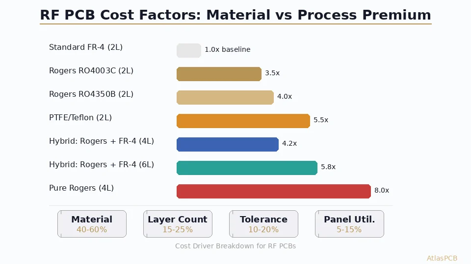
Rogers material costs $45-80 per square foot versus $8-12 for standard FR-4. For a typical 100x100mm board, Rogers material adds $5-15 per piece at prototype quantities. The most effective cost reduction strategies:
Hybrid stackup architecture reduces Rogers usage by 40-70%. Placing Rogers only on layers that carry RF signals (typically 1-2 cores in a 6+ layer build) cuts material cost dramatically while preserving RF performance where it matters.
Panel utilization — Rogers cores come in standard panel sizes (12x18” or 18x24”). Designing your board outline to maximize pieces per panel reduces per-unit material waste. A 50x80mm board fits 12 pieces on a 12x18” panel, but a 55x85mm board might only fit 9 — a 25% cost increase from 5mm of extra board space.
Core thickness selection — using standard catalog thicknesses (10, 20, 30, 60mil) avoids custom pressing charges. Non-standard thicknesses require Rogers to press specific lots, adding 4-6 weeks lead time and $500-2000 minimum order charges.
ATLASPCB
Start Your Rogers 4350B Project Today
Upload your design for a stackup recommendation tailored to your frequency, impedance targets, and budget. We stock RO4350B in common thicknesses for fast-turn delivery.
Upload Design Files ›Reviewed by AtlasPCB Engineering Team — 15+ years in advanced PCB fabrication for RF, HDI, and rigid-flex applications.
Related Reading:
About AtlasPCB — We specialize in complex PCB manufacturing for HDI, RF, and high-reliability applications. Explore our RF and high-frequency PCB services, or get an impedance-controlled PCB manufacturing . Every order includes free engineering review. Get your quote.
Reviewed by AtlasPCB Engineering Team — IPC-certified manufacturing specialists with 15+ years of production experience in HDI, RF, and high-reliability PCB fabrication. Content based on factory floor data and real customer design reviews.
- Rogers 4350B
- PCB stackup
- RF PCB
- hybrid stackup
- impedance controlled PCB
- high frequency PCB