· AtlasPCB Engineering · Engineering · 7 min read
AI-Driven Substrate Demand: How AI Chips Are Extending PCB Order Visibility to 2029
Kinsus Interconnect reports AI-driven substrate orders now extend visibility into 2028-2029. Analyze how CoWoS packaging expansion, HBM stacking, and the 1nm process transition are reshaping PCB substrate capacity planning and what this means for the broader supply chain.

The Substrate Capacity Lock-Up
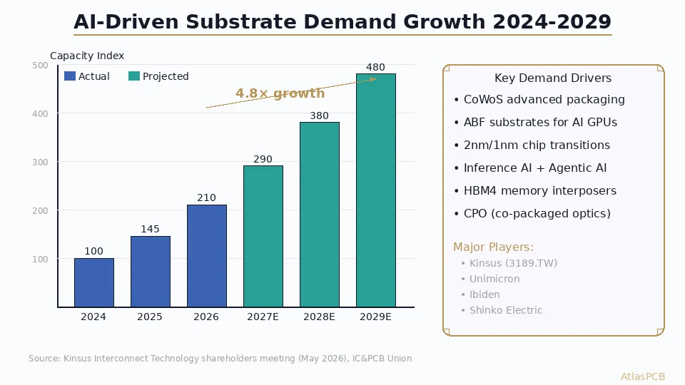
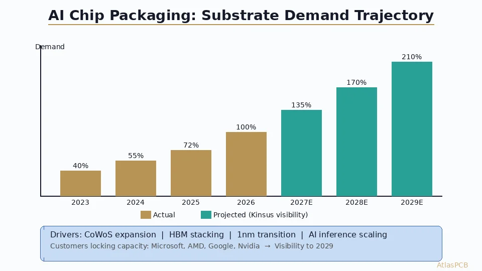
At its May 2026 annual shareholders meeting, Taiwanese PCB substrate maker Kinsus Interconnect Technology (3189.TW) revealed a striking data point: AI-driven demand has extended its substrate order visibility and capacity expansion planning into 2028 and 2029. Customers are no longer placing orders one or two quarters ahead — they’re locking in multi-year capacity commitments that fundamentally change how the substrate industry operates.
CEO Chen Ho-Hsu stated that the company’s ABF substrate business has already surpassed its previous 2022 peak, driven by the semiconductor industry’s transition toward sub-2nm processes and the continuing explosion in CoWoS advanced packaging demand. Director and Pegatron Chairman Tung Tzu-Hsien compared the current AI boom to the early 2000s internet revolution in its transformative impact on the supply chain.
This isn’t an isolated signal. Across the substrate industry, from Ibiden and Shinko in Japan to Samsung Electro-Mechanics in Korea, the same pattern emerges: AI customers securing multi-year supply agreements that leave other segments competing for remaining capacity.
Why AI Packaging Demands Extreme Substrates
The CoWoS Scale Challenge
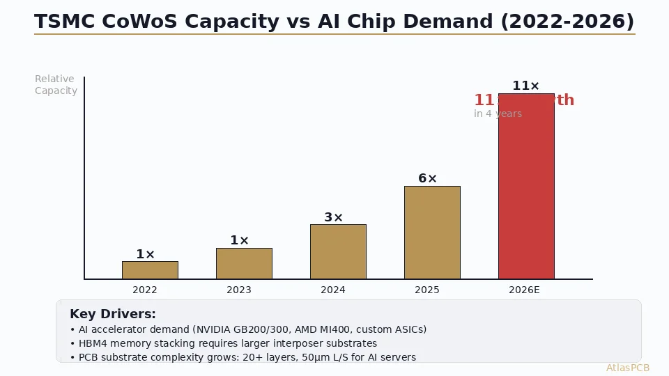
TSMC’s CoWoS (Chip-on-Wafer-on-Substrate) technology — used in Nvidia’s H100, H200, B100, and GB200 GPUs — requires interposer substrates of unprecedented size and complexity:
- Substrate area: Up to 5,500 mm² (6× reticle size) for latest generation
- Layer count: 12-20 layers in the substrate alone
- Line/space: 8/8 μm to 12/12 μm (compared to 30/30 μm for standard BGA substrates)
- Via density: >1 million microvias per substrate
- Warpage control: <100 μm across the entire substrate surface
Each generation of AI accelerator increases the substrate footprint. TSMC’s roadmap to CoWoS-L (using local silicon interconnect) and CoWoS with 11× reticle-size interposers demands substrates that push the boundaries of organic manufacturing technology.
HBM Stacking Creates Additional Demand
High Bandwidth Memory (HBM) — HBM3, HBM3E, and upcoming HBM4 — uses through-silicon vias (TSVs) to stack DRAM dies, but each HBM stack still requires a base substrate and integration into the main package substrate:
- Each AI GPU package contains 4-8 HBM stacks
- Each HBM stack requires its own substrate carrier
- The interposer substrate must accommodate all HBM stack sites plus the compute dies
- HBM4 with wider interfaces will increase substrate I/O density further
The 1nm Process Transition
As foundries move from 3nm to 2nm (TSMC N2, Intel 20A) and eventually 1nm, chip complexity and I/O density continue scaling:
- More transistors → more I/O pins → denser substrate routing
- Higher power density → more power delivery network (PDN) layers in substrate
- Chiplet architectures → multiple die mounting sites per substrate
- UCIe interconnects → ultra-fine-pitch substrate features between chiplets
Supply Chain Architecture for AI Substrates
The ABF Substrate Ecosystem
ABF substrates form a concentrated supply chain:
| Supplier | Market Share | Primary Customers | Capacity Status |
|---|---|---|---|
| Ibiden (Japan) | ~25% | Intel, Nvidia | Expanding aggressively |
| Shinko Electric (Japan) | ~20% | AMD, Intel | New Japan factory online 2027 |
| Kinsus (Taiwan) | ~15% | TSMC CoWoS, AMD | Expanding via technology-node approach |
| Unimicron (Taiwan) | ~12% | Apple, Qualcomm | Transitioning capacity to AI |
| Samsung E-M (Korea) | ~10% | Samsung, Nvidia | Building AI substrate lines |
The total addressable market for ABF substrates is projected to reach $18-20 billion by 2028, up from approximately $12 billion in 2025.
Technology-Node Expansion Strategy
Kinsus specifically described a “technology node” approach to capacity expansion rather than broad capacity buildout. This means investing in specific process capabilities (finer L/S, higher layer count, larger panel) rather than simply adding duplicate lines. The implication is clear: not all substrate capacity is fungible. Advanced AI substrates require fundamentally different manufacturing technology than standard IC substrates.
Customer Lock-In Dynamics
Microsoft, AMD, and Google are reportedly securing capacity directly from Taiwan’s substrate supply chain, according to industry sources cited alongside the Kinsus meeting. This creates a multi-layered lock-in:
- Equipment lead time: Substrate factory build-out takes 18-24 months
- Process qualification: New substrate processes require 6-12 months of qualification
- Material supply: ABF film supply from Ajinomoto is also capacity-constrained
- Engineering resources: Experienced substrate process engineers are scarce globally
Building AI Hardware? Secure Your PCB Substrate Capacity
AtlasPCB provides advanced multilayer PCBs for AI server power delivery, backplanes, and motherboard applications. Contact us early in your design cycle for capacity planning.
Discuss AI Hardware PCB Needs →Downstream Impact on Standard PCB Manufacturing
Material Competition
While advanced substrates use specialized materials (ABF film, ultra-thin copper foil, low-CTE core materials), several supply chain elements overlap with standard PCB production:
- Copper foil: Ultra-thin foil (<12 μm) demand from substrates competes with HDI PCB production
- Glass cloth: Special thin glass styles (106, 1035) used in both substrates and high-frequency PCBs
- Chemical supplies: Plating chemistry and desmear chemicals shared across the industry
- Clean room capacity: Substrate factories often share campus with advanced PCB facilities
Capacity Reallocation
Some substrate and HDI PCB manufacturers are actively reallocating capacity:
- Standard BT substrate lines converted to advanced AI substrate production
- Consumer electronics substrate capacity deprioritized in favor of AI products
- Legacy PCB manufacturing equipment sold to smaller firms as facilities upgrade
The result: even if your PCB doesn’t directly compete for substrate capacity, the broader ecosystem pressure affects material availability, skilled labor, and investment priorities throughout the supply chain.
Lead Time Implications
For hardware engineers designing AI-adjacent products (AI server racks, networking equipment, power systems), the implications are practical:
- Start capacity discussions earlier: 6+ months lead time for advanced HDI boards
- Second-source materials: Don’t single-source critical laminates
- Design for available materials: Verify material availability before specifying exotic laminates
- Panel utilization matters: Efficient panelization reduces capacity consumption
- Batch orders strategically: Larger, less frequent orders improve capacity planning
What This Means for PCB Design Engineers
Inference AI Expands Addressable Market
The AI substrate story isn’t just about training GPUs. As inference AI scales — particularly edge AI and agentic AI — the demand for high-end substrates diversifies beyond hyperscaler data centers:
- Edge AI processors: Smaller but still demanding packaging (10-14 layer substrates)
- Automotive AI: ADAS processors require automotive-grade substrates with extended reliability
- Telecom AI: Network processors for AI-powered routing and switching
- Industrial AI: Vision processors, robot controllers, predictive maintenance
Each application creates additional substrate demand pressure across different quality tiers.
Design Implications
For PCB designers working on boards that interface with or support AI hardware:
- Power delivery PCBs: AI server power stages require 20+ layer heavy-copper boards
- Backplanes: PCIe Gen5/6 backplanes need controlled impedance with tight tolerances
- Thermal solutions: Cold plate and heatsink mounting PCBs for liquid-cooled AI racks
- Network switches: 800G+ switch PCBs with ultra-low-loss materials
These boards, while not substrates themselves, face the same supply chain pressures and require advanced manufacturing capabilities.
The Road to 2029: Industry Outlook
Capacity Expansion Timeline
Based on announced investments:
- 2026: Existing expansion projects come online (Shinko, Ibiden, Samsung E-M)
- 2027: Next-generation substrate factories reach volume (Kinsus new facilities)
- 2028-2029: Demand visibility extends here, suggesting continued tight supply
- 2030+: Glass substrate technology may begin supplementing organic substrates for some applications (Intel’s glass substrate work targets this timeframe)
Technology Transitions on the Horizon
- Glass substrates: Better flatness and CTE match than organic, but still 4-5 years from volume production
- Silicon interposers: Continue scaling but limited by wafer-based manufacturing costs
- Fan-out packaging: Competes with CoWoS for some applications, uses different substrate technology
- Chiplet standardization (UCIe): Creates more predictable substrate interface requirements
Related Resources
- Glass core substrates for advanced packaging: The next generation of substrate technology
- AI hardware thermal management: Designing PCBs that support AI accelerators
- HDI PCB stackup design: Building multilayer boards for high-density applications
- TSMC CoWoS and PCB substrate convergence: How advanced packaging changes substrate requirements
Conclusion
The extension of substrate order visibility to 2028-2029 represents a structural shift in the electronics supply chain, not a temporary spike. AI’s insatiable appetite for compute translates directly into unprecedented demand for the advanced packaging substrates that connect silicon to system. For PCB professionals, this signals both challenges (material competition, lead time pressure, capacity constraints) and opportunities (growing market for AI-supporting boards, premium pricing for advanced capabilities, and long-term investment confidence in the industry).
The companies that adapt their capacity planning, material strategies, and manufacturing capabilities to serve the AI hardware ecosystem will capture disproportionate value in the coming years.
Supporting AI hardware with advanced PCBs? AtlasPCB manufactures high-layer-count boards with advanced materials for AI server power delivery, backplanes, and networking applications. Our capabilities include 24+ layer builds, controlled impedance, and heavy copper designs. Start a conversation →
About AtlasPCB — We specialize in complex PCB manufacturing for HDI, RF, and high-reliability applications. Explore our impedance-controlled PCB manufacturing . Every order includes free engineering review. Get your quote.
Reviewed by AtlasPCB Engineering Team — IPC-certified manufacturing specialists with 15+ years of production experience in HDI, RF, and high-reliability PCB fabrication. Content based on factory floor data and real customer design reviews.
- AI substrates
- ABF substrate
- PCB substrate demand
- CoWoS
- HBM
- Kinsus
- advanced packaging
- AI hardware
- capacity planning
- semiconductor