· AtlasPCB Engineering · Manufacturing · 13 min read
PCB Electroless Copper Plating: Chemistry, Process Steps, and Quality Control
Deep dive into PCB electroless copper plating — from palladium activation chemistry to deposition control, void prevention, and IPC standards for through-hole metallization.

The Invisible Foundation of Every PCB Through-Hole
Every multilayer PCB relies on through-hole connections — the copper-plated tunnels that carry signals and power between layers. These connections are so fundamental that it’s easy to take them for granted. But creating a reliable copper tube inside a hole drilled through fiberglass and resin is a remarkable feat of chemistry, and the most critical step in that process is one most engineers never think about: electroless copper plating.
Electroless copper is the thin seed layer — typically just 0.3-1.0μm thick — that transforms a non-conductive drilled hole into a surface that can accept electrolytic copper plating. Without this seed, copper won’t deposit on the fiberglass and resin exposed by drilling. Get the electroless copper wrong, and you get voids, delamination, barrel cracks, and interconnect failures that may not appear until the product is in the field.
This guide takes you through the complete electroless copper process: the chemistry, the process steps, the quality control methods, and the things that go wrong when process parameters drift.
Why Electroless Copper Is Necessary
The Drilling Problem
When a [PCB manufacturing process]/blog/pcb-manufacturing-process/) drills holes through a multilayer stackup, the drill bit cuts through alternating layers of copper foil and dielectric material (typically FR-4 fiberglass/epoxy). The resulting hole wall is a mosaic of copper rings (where the drill intersected copper layers) and exposed dielectric (fiberglass bundles and epoxy resin).
The copper rings are already conductive — they’re the edges of the internal copper layers. But the dielectric sections between them are insulators. To create a continuous electrical connection from top to bottom, those insulating sections must be made conductive. That’s the job of electroless copper.
Why Not Just Use Electrolytic Plating?
Electrolytic copper plating — the process that builds the final through-hole copper thickness — requires passing electrical current through the workpiece. Current flows through conductive surfaces, depositing copper ions from solution as metallic copper. But current can’t flow through insulators. If you immersed a drilled (but unmetallized) panel in an electrolytic copper bath, copper would deposit only on the existing copper surfaces (the foil on the outer layers and the exposed copper rings inside the holes), but not on the dielectric hole walls between those rings.
The result would be discontinuous copper — isolated rings with no connection between them. Electroless copper bridges those gaps by depositing a thin conductive layer on all exposed surfaces, including the dielectric, using chemical energy rather than electrical current.
The Chemistry of Electroless Copper
Electroless copper deposition is an autocatalytic reduction reaction. Once initiated on a catalytic surface, the reaction sustains itself as long as chemical reactants are available. The core chemistry:
The Reduction Reaction
Cu²⁺ + 2HCHO + 4OH⁻ → Cu⁰ + 2HCOO⁻ + 2H₂O + H₂↑
In plain terms: copper ions (Cu²⁺) from copper sulfate are reduced to metallic copper (Cu⁰) by formaldehyde (HCHO) in an alkaline environment. The reaction produces copper metal on the surface, formate ions as a byproduct, and hydrogen gas.
Bath Components
A typical electroless copper bath contains:
| Component | Typical Concentration | Function |
|---|---|---|
| Copper sulfate (CuSO₄) | 2-4 g/L (as Cu²⁺) | Copper source |
| Formaldehyde (HCHO) | 3-8 g/L | Reducing agent |
| EDTA or Tartrate | 20-40 g/L | Complexing agent (prevents Cu precipitation) |
| Sodium hydroxide (NaOH) | pH 12.0-13.0 | Alkalinity control |
| Stabilizers | Trace amounts | Prevent spontaneous decomposition |
| Surfactants/Wetting agents | Trace amounts | Improve hole wall wetting |
The complexing agent (EDTA — ethylenediaminetetraacetic acid — or potassium sodium tartrate) is essential. Without it, copper hydroxide would precipitate out of the alkaline solution, crashing the bath. The complexing agent keeps copper ions soluble while still allowing controlled reduction at catalytic surfaces.
Why Palladium?
The electroless copper reaction doesn’t start spontaneously on dielectric surfaces — it requires a catalyst. Palladium (Pd) serves this role. Palladium nanoparticles deposited on the hole wall surfaces during the activation step provide catalytic sites where formaldehyde oxidation and copper reduction can initiate. Once a thin layer of copper is deposited, the copper itself becomes catalytic (autocatalytic), and the reaction continues without the palladium.
The Complete Process Flow
Electroless copper plating is not a single step — it’s a sequence of carefully controlled chemical treatments. Each step prepares the surface for the next:
Step 1: Desmear
After drilling, the hole walls are contaminated with smeared resin — epoxy that was melted and dragged by drill friction. This smear layer must be removed to expose clean fiberglass and copper surfaces. [Plasma desmear]/blog/pcb-plasma-desmear-process/) or chemical (permanganate) desmear removes this layer and creates micro-roughness on the resin surface that improves adhesion.
Desmear quality directly determines electroless copper adhesion. Insufficient desmear is the number one root cause of [plating voids]/blog/pcb-plating-void-prevention/) in through-holes.
Step 2: Conditioning (Charge Modification)
The drilled and desmeared hole walls have variable surface charges — glass fibers are negatively charged, while resin may be neutral or slightly negative. The conditioner (typically a cationic polyelectrolyte) adsorbs onto the surface, creating a uniform positive charge that attracts the negatively charged palladium-tin colloidal particles in the next step.
Process parameters:
- Temperature: 40-50°C
- Immersion time: 3-5 minutes
- pH: 1.5-3.0 (acidic)
Step 3: Micro-Etch
A light chemical etch (typically sodium persulfate or hydrogen peroxide/sulfuric acid) removes oxide from the exposed copper ring surfaces inside the holes and on the panel surface. This creates a fresh, clean copper surface with micro-roughness that promotes adhesion of the subsequent palladium catalyst and electroless copper.
Critical control: Etch depth should be 1-2μm — enough to clean and roughen, not enough to undercut or thin the copper significantly.
Step 4: Pre-Dip (Catalyst Pre-Conditioning)
An acidic pre-dip (dilute hydrochloric acid or the carrier solution of the catalyst) prepares the surface and prevents dragout contamination of the catalyst bath. It also adjusts the pH of the surface solution film to match the catalyst bath conditions.
Step 5: Palladium-Tin Activation
This is the most critical step. A colloidal solution of palladium and tin (Pd/Sn colloid in hydrochloric acid) is applied to the panel. The colloidal particles — nanometer-scale Pd cores surrounded by Sn(II) hydroxide shells — adsorb onto all surfaces: copper, glass fiber, and resin.
Process parameters:
- Temperature: 20-30°C (room temperature common)
- Immersion time: 3-7 minutes
- Pd concentration: 100-250 ppm
- HCl concentration: 150-250 mL/L
- Tin concentration: 5-15 g/L
The Pd/Sn ratio and colloid stability are critical. Aging, contamination, or temperature excursions can destabilize the colloid, leading to incomplete activation and subsequent plating voids.
Step 6: Acceleration (Tin Stripping)
After activation, the tin hydroxide shell surrounding the palladium cores must be dissolved to expose the catalytic palladium surface. This is done in an accelerator solution — typically a dilute acid (fluoboric acid, hydrochloric acid, or organic acid).
The acceleration step converts the Pd/Sn colloid from:
Pd(core)/Sn(OH)₂(shell) → Exposed Pd nanoparticles
Insufficient acceleration leaves tin residue that inhibits copper deposition. Over-acceleration can strip palladium from the surface. Both conditions lead to voids.
Step 7: Electroless Copper Deposition
Finally, the activated and accelerated panel enters the electroless copper bath. The palladium catalytic sites initiate copper deposition, and the reaction propagates across the surface as deposited copper itself becomes catalytic.
Process parameters:
- Temperature: 30-45°C (most baths operate at 32-38°C)
- pH: 12.0-13.0
- Immersion time: 15-30 minutes (for 0.3-0.8μm deposit)
- Air agitation: Moderate (too vigorous introduces bubbles; too gentle causes stagnation)
- Bath loading: Controlled to prevent depletion
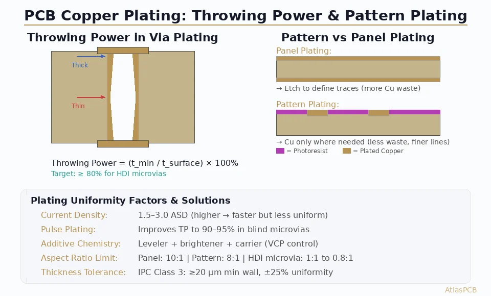
The deposition rate is typically 1-3μm per hour, though production processes target just 0.3-1.0μm — enough to provide a continuous conductive layer for subsequent [electrolytic copper plating]/blog/pcb-copper-plating-thickness-uniformity/).
Step 8: Anti-Tarnish / Micro-Etch
After electroless copper, a brief anti-tarnish or micro-etch treatment protects the freshly deposited copper from oxidation before the panel moves to electrolytic plating. Oxidized electroless copper has poor adhesion to the subsequent electrolytic deposit.
Process Control: What Goes Wrong
Electroless copper is arguably the most chemistry-sensitive step in the entire [PCB manufacturing process]/blog/pcb-manufacturing-process/). Small deviations in bath chemistry or process parameters can cause catastrophic quality failures:
Void Formation
Voids in the electroless copper layer — areas where no copper deposited — are the most common and most serious defect. Voids propagate through the subsequent electrolytic copper, creating discontinuities in the through-hole barrel that may pass initial electrical testing but fail under thermal stress.
Root causes:
- Insufficient desmear (resin residue prevents catalyst adsorption)
- Poor activation (inadequate Pd coverage, destabilized colloid)
- Air entrapment (bubbles trapped in holes block solution access)
- Bath chemistry imbalance (low formaldehyde, incorrect pH)
- Contamination (organic contaminants poison the catalyst)
Detection: Cross-section microsection analysis per [IPC-6012]/blog/ipc-standards-pcb-classes/) Section 3.6 — minimum electroless copper coverage requirements.
Bath Decomposition
The electroless copper bath is thermodynamically unstable — the reduction reaction would spontaneously decompose the entire bath if not controlled by stabilizers. Bath decomposition occurs when:
- Temperature exceeds limits (runaway exothermic reaction)
- Stabilizer concentration drops below threshold
- Excessive catalytic surface area (overloaded bath)
- Contamination introduces catalytic particles
A decomposed bath deposits copper randomly (on tank walls, pipes, filters) rather than selectively on the workpiece. Bath decomposition is a batch-killing event that requires draining, cleaning, and rebuilding the bath.
Poor Adhesion
Even when copper deposits uniformly, it may not adhere well to the hole wall. Poor adhesion manifests as:
- Copper lifting during subsequent processing (lamination, thermal cycling)
- Barrel cracks during thermal stress testing
- [Plated-through-hole reliability]/blog/pcb-plated-through-hole-reliability/) failures in field service
Root causes: Insufficient surface roughness from desmear, contamination between process steps, inadequate micro-etch, excessive delay between steps allowing surface oxidation.
Thickness Variation
Electroless copper thickness should be uniform across the panel and within each hole. Significant variation indicates process problems:
- Hole-to-hole variation: Different hole diameters experience different flow dynamics, with smaller holes potentially receiving less solution exchange and thinner deposits
- Top-to-bottom variation within holes: Gravity and solution flow patterns can create thinner deposits at hole midpoints, especially in [high-aspect-ratio holes]/blog/pcb-aspect-ratio-via-design/)
- Panel-position variation: Edge effects and agitation patterns can cause panels to have thicker deposits at edges versus center
Alternatives to Electroless Copper
While electroless copper remains the dominant through-hole metallization method, alternatives exist:
Direct Metallization
Direct metallization processes (carbon-based or conductive polymer-based) skip the palladium activation and electroless copper steps entirely. Instead, they deposit a conductive (but non-metallic) layer directly on the desmeared hole wall:
- Carbon direct metallization: Colloidal carbon particles coat the hole wall, providing conductivity for electrolytic plating
- Conductive polymer: Polymerized conductive coating (e.g., polypyrrole) serves as the seed layer
Advantages: Eliminates formaldehyde (environmental benefit), fewer process steps, no bath decomposition risk, lower palladium costs.
Disadvantages: Lower conductivity than electroless copper (higher resistance seed layer), potential adhesion challenges with some substrate materials, may not be suitable for [high-reliability applications]/blog/pcb-reliability-testing/) requiring IPC Class 3 compliance.
Direct metallization has gained significant market share in the past decade, particularly for standard multilayer boards. However, electroless copper remains preferred for HDI and high-reliability applications where maximum plating quality is required.
Black Hole and Shadow Processes
These are specific implementations of direct metallization:
- Black Hole: MacDermid’s carbon-based process
- Shadow: Enthone’s graphite dispersion process
Both create a thin conductive layer through carbon/graphite particle adsorption rather than chemical copper deposition.
Quality Control and Testing
In-Process Monitoring
Critical parameters monitored during electroless copper production:
| Parameter | Method | Frequency | Target |
|---|---|---|---|
| Copper concentration | Titration (iodometric) | Every 2-4 hours | 2-4 g/L |
| Formaldehyde | Titration (sulfite) | Every 2-4 hours | 3-8 g/L |
| EDTA | Titration | Daily | 20-40 g/L |
| pH | pH meter | Continuous | 12.0-13.0 |
| Temperature | Thermocouple | Continuous | 32-38°C |
| Specific gravity | Hydrometer | Daily | Monitor for buildup |
| Deposition rate | Coupon weight gain | Per shift | 1-3 μm/hr |
Post-Process Inspection
- Backlight test: Illuminate hole from one side, inspect from opposite — any light leakage indicates voids
- Microsection analysis: Cross-section through representative holes, measure electroless copper thickness and coverage under metallurgical microscope
- Thermal stress test: Float coupon on 288°C solder for 10 seconds, microsection for cracks (per IPC-TM-650 2.6.8)
- Electrical continuity: [Flying probe or fixture testing]/blog/pcb-electrical-testing-flying-probe-vs-fixture/) to verify all connections
IPC Requirements
IPC-6012 specifies minimum requirements for through-hole copper plating:
| Parameter | IPC Class 2 | IPC Class 3 |
|---|---|---|
| Minimum hole wall copper | 20μm average | 25μm minimum |
| Maximum voids | 1 void, max 5% circumference | No voids allowed |
| Plating adhesion | Must survive thermal stress | Must survive thermal stress × 3 cycles |
Note that these are total copper thickness requirements (electroless + electrolytic). The electroless layer itself is typically 0.3-1.0μm and is included in the total measurement.
Impact on Downstream Processes
The quality of the electroless copper deposit directly affects every subsequent manufacturing step:
Electrolytic Copper Plating
The electroless copper provides the conductive base for [electrolytic plating]/blog/pcb-copper-plating-thickness-uniformity/). A uniform, well-adhered electroless layer produces uniform electrolytic deposit. Voids or poor adhesion in the electroless layer propagate through the electrolytic copper — they cannot be “healed” by subsequent plating.
Via Fill Plating
For [via-in-pad plated over (VIPPO)]/blog/pcb-via-in-pad-plated-over-design/) and blind via fill applications, the electroless copper quality on the via bottom is critical. The via bottom is the most challenging area for electroless coverage because:
- It’s the furthest point from solution exchange
- Desmear residue tends to accumulate at the bottom
- Air bubbles are most likely to be trapped at the bottom of blind vias
HDI manufacturers pay particular attention to electroless copper quality on [blind via bottoms]/blog/pcb-blind-via-fill-technology/) because void-free fill plating depends on complete electroless coverage.
Reliability
Through-hole reliability under thermal cycling — the primary reliability concern for multilayer PCB manufacturers — depends fundamentally on the adhesion and continuity of the electroless copper to the hole wall. During thermal cycling, differential expansion between copper (CTE ~17 ppm/°C) and FR-4 Z-axis (CTE ~50-70 ppm/°C above Tg) stresses the plated copper barrel. Any void or adhesion weakness in the electroless layer becomes a crack initiation site.
This is why [IPC Class 3 requirements]/blog/ipc-standards-pcb-classes/) specify zero voids in through-hole plating — a standard that demands exceptional electroless copper process control.
Practical Considerations for PCB Designers
While electroless copper is primarily a manufacturing process, designers can influence its success:
Aspect Ratio Limits
High [aspect ratio holes]/blog/pcb-drilling-aspect-ratio-limits/) (depth-to-diameter ratio greater than 8:1) are more difficult to plate because solution exchange in deep, narrow holes is limited. This affects both electroless and electrolytic copper deposition. Design holes within your fabricator’s proven aspect ratio capability.
Hole Size Uniformity
Boards with a wide range of hole sizes (e.g., 0.2mm microvias and 3.0mm mounting holes on the same panel) create process optimization challenges. The electroless process parameters optimized for small holes may not be optimal for large holes, and vice versa. Discuss mixed-hole designs with your PCB manufacturer during the design phase.
Material Selection
Some substrate materials are more challenging for electroless copper adhesion. [PTFE-based materials]/blog/ptfe-substrate-handling-fabrication/) used in RF applications, for example, have poor natural adhesion to deposited copper and require specialized desmear and surface preparation processes. [High-Tg materials]/blog/high-tg-pcb-material-selection/) may also require adjusted desmear parameters.
Summary
Electroless copper plating is the invisible but essential foundation of PCB through-hole connectivity. The process transforms insulating hole walls into conductive surfaces through a precisely controlled sequence of chemical treatments — desmear, conditioning, activation, acceleration, and copper deposition. Each step builds on the previous one, and each has failure modes that can compromise the final product.
For PCB designers, the key takeaways are:
- Aspect ratio matters — higher ratios are harder to plate reliably
- Material choice affects plating — discuss non-standard materials with your fab early
- Via-in-pad requires premium plating quality — specify [IPC Class 3]/blog/ipc-standards-pcb-classes/) if via fill reliability is critical
- Through-hole reliability depends on electroless quality — it all starts with the seed layer
For manufacturers, electroless copper process control is one of the most significant differentiators between fabricators that deliver reliable multilayer PCBs and those that struggle with yield and field failures. Investment in monitoring, analytical equipment, and operator training pays dividends in plating quality that echoes through every board produced.
Ready to optimize your PCB design? Upload your Gerbers for a free engineering review from our team.
Further Reading
- [Rogers PCB Fabrication: Material Sourcing, Lead Times & Quality Control]/blog/rogers-pcb-fabrication/)
- [PCB Rigid-Flex Bend Zone Reliability: Design Rules, Material Selection & Lifecycle Testing]/blog/pcb-rigid-flex-bend-zone-reliability/)
- [ENEPIG vs ENIG Surface Finish: Complete Comparison for Wire Bonding, Solderability, and Long-Term Reliability]/blog/enepig-vs-enig-surface-finish-wire-bonding/)
- [PCB Surface Finish Comparison: OSP vs HASL vs Immersion Silver vs ENIG for Assembly Reliability]/blog/pcb-surface-finish-osp-hasl-enig-immersion-silver-comparison/)
- [PCB Manufacturer with Engineering Review: Why Human DFM Audit Matters]/blog/pcb-manufacturer-engineering-review/)
- Our Manufacturing Capabilities
About AtlasPCB — We specialize in complex PCB manufacturing for HDI, RF, and high-reliability applications. Explore our full PCB manufacturing capabilities . Every order includes free engineering review. Get your quote.
Reviewed by AtlasPCB Engineering Team — IPC-certified manufacturing specialists with 15+ years of production experience in HDI, RF, and high-reliability PCB fabrication. Content based on factory floor data and real customer design reviews.
- electroless copper
- plating
- manufacturing
- through-hole
- metallization
- PCB manufacturing