· AtlasPCB Engineering · Engineering · 14 min read
PCB Copper Plating: Thickness Uniformity, Specifications, and Quality Control
A comprehensive guide to PCB copper plating processes, including electroless and electrolytic plating, thickness uniformity challenges, IPC-6012 specifications, pulse plating technology, and plating void prevention strategies for reliable multilayer boards.
PCB Copper Plating: Thickness Uniformity, Specifications, and Quality Control
Copper plating is one of the most critical processes in PCB manufacturing. It creates the electrical connections between layers through plated through-holes (PTH), builds up surface copper for trace routing, and forms the conductive barrels that must survive thermal cycling, soldering, and years of service life. When copper plating fails — through insufficient thickness, poor adhesion, voids, or non-uniform deposition — the board fails.
Despite its importance, copper plating is one of the least understood processes among PCB designers. Most engineers specify a copper weight (1 oz, 2 oz) and assume the fabricator handles the rest. But understanding plating fundamentals helps you make better design decisions: why certain via aspect ratios are difficult, why minimum annular ring requirements exist, and why your fabricator might push back on aggressive HDI designs.
This article covers the complete copper plating process — from electroless seed layer through final electrolytic buildup — with emphasis on thickness uniformity, IPC specifications, and the quality control methods that ensure reliable boards.
The Two-Stage Plating Process
PCB copper plating is a two-stage process. Each stage serves a distinct purpose and has its own chemistry, equipment, and failure modes.
Stage 1: Electroless Copper Deposition
After drilling, the exposed dielectric material in through-holes and blind vias is non-conductive. Before electrolytic plating can occur, a thin conductive seed layer must be deposited through a chemical (electroless) process. This is sometimes called “chemical copper” or “autocatalytic copper.”
The electroless copper process follows these steps:
1. Desmear / Etchback. Drilling generates heat that smears resin across the inner-layer copper connections in the hole wall. This resin smear must be removed to ensure reliable copper-to-copper interconnection. The standard process uses a three-step chemical desmear: solvent swell (N-methylpyrrolidone or equivalent), permanganate etch (potassium permanganate oxidizes and removes resin), and neutralization (acid bath to remove permanganate residue and MnO₂). For high-reliability applications (IPC-6012 Class 3), a controlled etchback of 0.5–1.0 mil removes additional resin and creates a “three-point connection” where the electroless copper wraps around the exposed inner-layer copper edge.
2. Conditioning / Catalyzing. The hole wall surface is treated with a conditioner (cationic surfactant) that promotes uniform adhesion of the palladium catalyst. Then a colloidal palladium-tin catalyst solution is applied, depositing microscopic palladium particles on the dielectric surface. These particles serve as nucleation sites for the electroless copper reaction.
3. Acceleration. A dilute acid bath removes the tin component from the palladium-tin colloid, exposing the pure palladium catalyst particles and making them reactive.
4. Electroless Copper Deposition. The activated panels are immersed in the electroless copper bath — an alkaline solution containing copper sulfate, formaldehyde (reducing agent), sodium hydroxide, and complexing agents (typically EDTA or Rochelle salt). The formaldehyde reduces copper ions to metallic copper on the palladium catalyst sites. The reaction is:
Cu²⁺ + 2HCHO + 4OH⁻ → Cu⁰ + 2HCOO⁻ + 2H₂O + H₂
This deposits a uniform copper layer of 0.5–1.5 µm (20–60 microinches) on all non-conductive surfaces in the holes. The layer is thin, porous, and insufficient for service — but it provides the electrical conductivity needed for the subsequent electrolytic plating stage.
Critical Quality Parameters:
- Bath temperature: typically 30–36°C (higher accelerates deposition but reduces bath stability)
- Copper-to-formaldehyde ratio: must be maintained within tight limits to prevent bath decomposition
- pH: 12.0–13.0 (critical for reaction rate and deposit quality)
- Deposition time: 15–30 minutes depending on target thickness
Stage 2: Electrolytic Copper Plating
With the electroless seed layer providing conductivity, the panels move to electrolytic plating — an electrochemical process that deposits the bulk of the copper thickness. The panel (cathode) is immersed in an acid copper sulfate bath with copper anode bars, and DC current drives copper ions from solution onto the panel surface and into the holes.
The standard acid copper plating bath contains:
- Copper sulfate (CuSO₄·5H₂O): 60–80 g/L Cu²⁺ — provides the copper ions
- Sulfuric acid (H₂SO₄): 180–240 g/L — provides conductivity and controls throwing power
- Chloride ions: 40–80 ppm — essential for leveler additive function
- Organic additives (proprietary blends from suppliers like Atotech, MacDermid Alpha, DOW):
- Brightener (accelerator): bis-(3-sulfopropyl)-disulfide (SPS) or similar — increases deposition rate in recesses
- Carrier (suppressor): polyethylene glycol (PEG) or polypropylene glycol (PPG) — suppresses deposition on exposed surfaces
- Leveler: nitrogen-containing polymers — provides additional suppression at high-current-density areas
The interplay between these three additive classes is what enables uniform plating in high-aspect-ratio holes. The suppressor adsorbs preferentially on flat surfaces (high current density areas), slowing deposition there, while the accelerator concentrates in recessed areas (hole centers), speeding deposition there. The net effect is more uniform copper distribution between surface and hole interior.
For a deeper understanding of how copper weight translates to physical thickness, see our guide on [PCB copper weight and thickness]/blog/pcb-copper-weight-thickness/).
Thickness Uniformity: The Core Challenge
Achieving uniform copper plating thickness across an entire panel — and especially between the panel surface and the through-hole interiors — is the central challenge in PCB plating.
Why Uniformity Is Difficult
Current density distribution is inherently non-uniform in electrolytic plating. Areas closer to the anode, edges of the panel, and exposed surface areas receive higher current density than recessed areas like hole interiors. Without compensation, the surface would plate 2–3× thicker than the hole center.
Several factors affect uniformity:
Aspect ratio. The ratio of board thickness to hole diameter directly determines plating difficulty. A 1.6 mm board with 0.3 mm holes (aspect ratio 5.3:1) is significantly harder to plate uniformly than the same board with 0.5 mm holes (aspect ratio 3.2:1). Industry standard capability is around 8:1 for standard processes; advanced processes reach 12–15:1.
Panel position effects. Panels closer to the anode center plate thicker than those at the edges. Within a single panel, areas near the panel edge plate thicker than the center due to electric field concentration at edges (the “dog bone” effect). Thief patterns (non-functional copper features) around the panel border help equalize current distribution.
Pattern density. Areas with dense copper features (many traces and pads) consume more current locally, potentially starving adjacent areas. Large open areas of copper plate faster than fine-pitch traces surrounded by non-copper. This is one reason fabricators prefer uniform copper distribution in your design — it makes plating uniformity achievable.
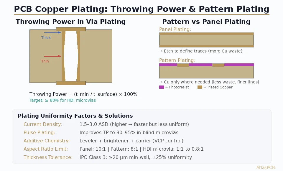
Measuring Throwing Power
Throwing power (TP) quantifies a plating bath’s ability to deposit copper uniformly into holes. It is typically measured using a Haring cell or by cross-sectioning plated through-holes and measuring the ratio of copper thickness at the hole center versus the surface:
TP(%) = (Thickness at hole center / Thickness at surface) × 100
Modern high-throwing-power acid copper baths achieve TP values of 70–85% for standard aspect ratios (≤8:1). For a target surface plating of 25 µm, this means the hole center receives 17.5–21.3 µm — within IPC-6012 Class 2 requirements but potentially tight for Class 3.
For high-aspect-ratio holes (>10:1), throwing power drops significantly, often to 50–60%, necessitating additional process controls or alternative plating techniques.

IPC-6012 Copper Plating Requirements
IPC-6012 “Qualification and Performance Specification for Rigid Printed Boards” defines the minimum requirements for copper plating quality. Understanding these specifications helps you communicate requirements to your fabricator and evaluate cross-section quality reports.
Through-Hole Plating Thickness
| Parameter | Class 1 (General) | Class 2 (Dedicated Service) | Class 3 (High Reliability) |
|---|---|---|---|
| Average PTH copper | ≥20 µm (0.8 mil) | ≥20 µm (0.8 mil) | ≥25 µm (1.0 mil) |
| Minimum any point | ≥15 µm (0.6 mil) | ≥18 µm (0.7 mil) | ≥20 µm (0.8 mil) |
| Voids allowed | Minor | Minor | None |
| Etchback (if specified) | — | — | 0.5–3.0 mil |
| Wicking (max) | — | 3.0 mil | 1.0 mil |
These measurements are taken from microsectioned cross-sections — destructive testing where a plated through-hole is cut in half, polished, and examined under a metallurgical microscope at 100–500× magnification.
Surface Copper
Surface copper after plating must meet the specified weight plus plating addition. For a 1 oz (35 µm) base copper with 25 µm plating, the total surface copper should be approximately 60 µm. IPC-6012 requires surface copper thickness to be within the specified tolerance, which varies by class.
Inner-Layer Connection Quality
The connection between the plated through-hole barrel and the inner-layer copper pad is critical. IPC-6012 specifies:
- No voids at the interconnection (all classes)
- Minimum interconnect defect (void, crack, or separation) per Class: Class 2 allows minor defects totaling no more than a certain angular portion; Class 3 allows essentially zero defects
- Etchback/wicking requirements — Class 3 typically requires controlled etchback to ensure the electroless copper wraps around the inner-layer copper edge, creating a “three-point connection” that dramatically improves interconnect reliability
For related information on via reliability testing methods, see our guide on [PCB via reliability testing]/blog/pcb-via-reliability-testing/).
Pulse Plating: Advanced Uniformity Control
Conventional DC plating uses a constant current throughout the process. Pulse plating alternates between high-current pulses and off-time (or reverse-current pulses), providing several advantages for uniformity:
How Pulse Plating Works
Instead of a steady 20 ASF (amps per square foot) DC current, a pulse plating system applies:
- Forward pulse: High current (e.g., 40 ASF) for 10–50 milliseconds
- Off-time or reverse pulse: Zero current or low reverse current (e.g., -5 ASF) for 1–10 milliseconds
During the forward pulse, copper deposits rapidly. During the off-time, copper ions in the depleted diffusion layer near the cathode surface replenish from the bulk solution. In reverse pulse mode, a small amount of copper is preferentially dissolved from high-current-density areas (surface and hole corners), effectively redistributing the deposit.
Pulse Plating Benefits
Improved throwing power. Pulse plating typically improves throwing power by 10–15 percentage points compared to DC plating with the same bath chemistry. A bath achieving 75% TP with DC may reach 85–90% TP with optimized pulse parameters.
Finer grain structure. Copper deposited by pulse plating has a finer crystalline grain structure than DC deposits, resulting in:
- Higher tensile strength (300–400 MPa vs 200–300 MPa for DC)
- Better ductility (elongation 12–18% vs 8–15% for DC)
- Improved thermal shock resistance
Reduced additive consumption. The off-time/reverse pulses allow additive replenishment at the cathode surface, reducing overall additive consumption and improving bath life.
Pulse Reverse Plating (PPR)
The most advanced variant, periodic pulse reverse (PPR) plating, uses a carefully timed sequence of forward and reverse current pulses. PPR can achieve throwing power exceeding 90% in high-aspect-ratio holes and is increasingly used for HDI manufacturing where via aspect ratios of 10:1 or higher are common.
Plating Void Prevention
Plating voids — discontinuities in the copper barrel — are among the most serious defects in PCB manufacturing. A void creates a weak point that can crack under thermal stress, leading to intermittent open circuits that are extremely difficult to diagnose in the field.
Common Causes of Plating Voids
1. Inadequate desmear. The most frequent root cause. If resin smear remains on the hole wall after desmear, the electroless copper cannot nucleate on those areas, leaving bare spots that become voids after electrolytic plating.
Indicators: Voids concentrated at inner-layer interfaces; voids that follow the drill smear pattern.
Prevention: Optimize permanganate concentration, temperature, and dwell time. Verify desmear effectiveness with backlight testing (shining light through plated holes to detect thin spots).
2. Poor electroless copper coverage. If the palladium catalyst doesn’t deposit uniformly — due to contaminated conditioner, insufficient activation time, or expired catalyst — some areas of the hole wall will not receive the electroless seed layer.
Indicators: Random void distribution; voids not correlated with inner-layer positions.
Prevention: Monitor catalyst bath activity with coupons; replace baths at recommended intervals; verify rinse water quality (DI water, <5 µS/cm conductivity).
3. Air entrapment. Air bubbles trapped in holes during plating physically block copper deposition. This is particularly problematic for small-diameter or high-aspect-ratio holes where surface tension holds air bubbles in place.
Indicators: Voids in the hole center, often elongated along the hole axis.
Prevention: Use solution agitation (air sparging, eductor nozzles, or panel oscillation) designed to dislodge bubbles from holes. Pre-wet panels before plating. Consider vacuum pre-treatment for high-aspect-ratio boards.
4. Excessive current density. Plating at too-high current density causes hydrogen gas evolution at the cathode, which can create gas pockets that block copper deposition and produce nodular, rough deposits.
Indicators: Rough, nodular plating with scattered voids; “burned” appearance near panel edges.
Prevention: Optimize current density for the specific board design and aspect ratio. Use current density ramp-up (start at 5–10 ASF, ramp to 15–25 ASF over 5–10 minutes).
5. Contaminated bath chemistry. Organic contaminants (photoresist residue, conveyor lubricants, breakdown products), metallic impurities (iron, tin, lead), and chloride imbalance all degrade plating quality.
Prevention: Regular Hull cell testing, CVS (cyclic voltammetric stripping) analysis of additive levels, activated carbon treatment for organics, and strict drag-in controls.
Quality Control Methods
Cross-Section Analysis
The gold standard for plating quality verification. Test coupons containing representative through-holes are microsectioned — cross-cut with a diamond saw, mounted in epoxy, ground and polished to the hole center, then examined under a metallurgical microscope.
Cross-section analysis reveals:
- Copper thickness at multiple points (surface, hole entrance, hole center, knee)
- Void presence and location
- Inner-layer connection quality
- Etchback depth
- Grain structure and deposit quality
IPC-6012 requires cross-section analysis as part of qualification testing and periodic production verification.
Backlight Testing
A rapid, non-destructive screening method. Light is directed through plated through-holes; voids or thin spots allow more light through, appearing as bright spots when viewed from the opposite side. This method catches gross plating defects but cannot measure thickness quantitatively.
Four-Point Probe Measurement
Surface copper thickness is measured non-destructively using a four-point probe (or eddy current gauge). These measurements verify that the surface plating meets thickness targets but cannot assess hole-wall plating.
Thermal Stress Testing
Per IPC-TM-650, Method 2.6.8, plated through-holes are subjected to thermal stress (solder float at 288°C for 10 seconds, repeated 3–6 times) followed by cross-section analysis. This tests whether the plating can survive assembly and rework without cracking or delamination. IPC-6012 Class 3 requires survival of 6 solder float cycles.
For more on how these quality control steps integrate into the broader multilayer manufacturing process, see our detailed overview of [multilayer PCB manufacturing]/blog/multilayer-pcb-manufacturing-process-explained/).
Design Recommendations for Plating Success
Understanding plating limitations helps you create designs that manufacture reliably:
Keep aspect ratios reasonable. Standard processes handle 8:1 reliably. If your design requires higher aspect ratios, discuss capabilities with your fabricator before finalizing.
Avoid extreme via size variation on the same board. A board with both 0.15 mm and 1.0 mm holes creates a plating dilemma — current density optimized for small holes overplates large holes, and vice versa.
Maintain uniform copper density. Large copper-free areas adjacent to dense copper areas create plating non-uniformity. Use copper fill (hatched or solid) in open areas to equalize current distribution.
Specify the right IPC class. Don’t default to Class 3 unless your application requires it. Class 3 specifications add cost through tighter process controls, etchback requirements, and more extensive testing. Class 2 is appropriate for the vast majority of commercial, industrial, and even many military applications.
Consider annular ring budget. Plating adds copper to both the hole wall and the pad. A 0.3 mm drilled hole with 25 µm plating becomes effectively 0.25 mm finished. Ensure your annular ring calculations account for this plating intrusion.
Communicate critical features. If certain vias are reliability-critical (e.g., BGA escape vias that will undergo multiple reflow cycles), note them in your fabrication drawing. The fabricator can prioritize plating quality monitoring on those features.
Conclusion
Copper plating transforms a stack of insulating layers and copper foils into a functioning, interconnected PCB. The process is conceptually simple — deposit a seed layer, then electroplate to build up thickness — but achieving consistent quality across millions of holes per production lot requires sophisticated chemistry, precise process control, and rigorous quality verification.
For designers, the key takeaway is that plating uniformity is a function of your design choices as much as the manufacturer’s process capability. Reasonable aspect ratios, uniform copper density, and appropriate IPC class specifications set your fabricator up for success. When in doubt, engage your manufacturer early — a five-minute conversation about via sizes during the design phase prevents expensive re-spins after bare board testing reveals plating issues.
Ready to start your project? Upload your Gerbers for a free engineering review, or talk to an engineer about your design requirements.
Further Reading
- [Rogers PCB Fabrication: Material Sourcing, Lead Times & Quality Control]/blog/rogers-pcb-fabrication/)
- [PCB Manufacturer with Engineering Review: Why Human DFM Audit Matters]/blog/pcb-manufacturer-engineering-review/)
- [ENEPIG vs ENIG: Which PCB Surface Finish for Your Design?]/blog/enepig-vs-enig/)
- [PCB Surface Finish Selection — ENIG vs HASL vs OSP vs Hard Gold vs ENEPIG]/blog/pcb-surface-finish-enig-hasl-osp-hard-gold-enepig/)
- [Medical PCB Manufacturing: FDA Compliance, Traceability & Reliability]/blog/medical-pcb-manufacturing-requirements/)
- Our Manufacturing Capabilities
About AtlasPCB — We specialize in complex PCB manufacturing for HDI, RF, and high-reliability applications. Explore our full PCB manufacturing capabilities . Every order includes free engineering review. Get your quote.
Reviewed by AtlasPCB Engineering Team — IPC-certified manufacturing specialists with 15+ years of production experience in HDI, RF, and high-reliability PCB fabrication. Content based on factory floor data and real customer design reviews.
- copper-plating
- thickness-uniformity
- pcb-manufacturing
- quality-control
- ipc-6012