· AtlasPCB Engineering · Engineering · 15 min read
Plating Void Prevention in PCB Vias
Causes, detection methods, and process controls for preventing plating voids in PCB through-hole and microvia plating.
Introduction: Why Plating Voids Matter
The plated through-hole (PTH) via remains one of the most critical interconnection structures in printed circuit board fabrication. Each via must provide reliable electrical continuity and thermal conductivity between copper layers through a barrel of electroplated copper typically 20–35 µm thick. A plating void — any localized area where this copper barrel is absent, thinned, or discontinuous — represents a latent reliability risk that can manifest as intermittent opens, increased via resistance, or catastrophic failure under thermal stress.
The consequences scale with the application. In consumer electronics, a plating void may cause a warranty return. In automotive electronics operating at 150°C junction temperatures with 15-year life requirements, it causes a field failure. In aerospace and defense systems, it can cause a mission-critical malfunction. Industry data from IPC and major OEMs consistently identifies plating voids among the top five PCB fabrication defect modes, accounting for 8–15% of all board failures in reliability testing.
This article provides a comprehensive technical examination of plating void mechanisms, detection methods, process controls, and prevention strategies for PCB manufacturers and designers seeking to maximize via reliability.
For related quality topics, see our articles on [PCB via reliability testing]/blog/pcb-via-reliability-testing/) and [common PCB defects prevention]/blog/common-pcb-defects-prevention/).
Anatomy of a Plating Void
Via Plating Process Overview
Understanding plating voids requires understanding the plating process sequence. After drilling, a via hole passes through several chemical and electrochemical processes:
- Deburring — Mechanical or chemical removal of drill burrs from entry and exit surfaces
- Desmear — Chemical or plasma removal of resin smear from drilled hole walls
- Etchback (optional) — Controlled removal of resin to expose inner-layer copper surfaces
- Conditioning — Surface preparation to promote catalyst adhesion
- Catalyzation — Deposition of palladium-tin catalyst seeds onto non-conductive hole wall surfaces
- Electroless copper — Chemical (autocatalytic) deposition of a thin copper seed layer (0.3–1.0 µm)
- Electrolytic copper — Electrochemical plating of the structural copper layer (20–35 µm)
- Post-treatment — Rinsing, anti-tarnish, and surface finishing
A plating void can originate at any stage in this sequence, but the root cause is most commonly traceable to steps 2–6.
Types and Locations of Plating Voids
| Void Type | Typical Location | Primary Cause | Cross-Section Appearance |
|---|---|---|---|
| Barrel void | Mid-barrel, away from pads | Air bubble entrapment during electroplating | Circular or elongated gap in barrel wall |
| Corner void | Junction of barrel and inner-layer pad | Incomplete desmear; insufficient etchback | Wedge-shaped gap at interconnect |
| Seed layer void | Random locations on hole wall | Electroless copper skip-plating | Thin or absent copper over bare substrate |
| Interconnect void | Inner-layer connection point | Drill smear residue blocking bonding | Gap between barrel plating and innerlayer copper |
| Fold void | Near entry/exit surface | Foil fold-over during lamination | Crescent-shaped void near surface |
| Nodule void | Adjacent to copper nodules | Plating bath contamination | Void behind or beneath copper nodule |
The most reliability-critical void types are interconnect voids and barrel voids, as they directly compromise the electrical and thermal path through the via.
Root Causes and Mechanisms
Drill Smear and Inadequate Desmear
When a drill bit passes through a multilayer PCB, frictional heat softens and smears epoxy resin across exposed inner-layer copper surfaces. This “drill smear” creates an insulating barrier that prevents both electroless seed deposition and electrolytic copper bonding at interconnect locations.
Contributing factors:
- Drill bit wear (>3,000 hits on a single bit for FR-4)
- Excessive drill feed rate or spindle speed generating excessive heat
- High resin content prepreg materials (>65% resin content)
- Improper backup material allowing excessive heat buildup
Desmear process requirements:
| Parameter | Permanganate Desmear | Plasma Desmear |
|---|---|---|
| Mechanism | Chemical oxidation of resin | Physical/chemical ablation by reactive ions |
| Typical chemistry | KMnO₄ (55–65 g/L) + NaOH | CF₄/O₂ gas mixture |
| Temperature | 75–85°C | 40–80°C (plasma chamber) |
| Process time | 8–15 minutes | 10–30 minutes |
| Etchback capability | Moderate (3–8 µm) | Excellent (1–25 µm controllable) |
| Hole size range | >0.2 mm effectively | All sizes; superior for <0.2 mm |
| Resin type compatibility | FR-4, polyimide | All resin systems including PTFE |
Incomplete desmear — whether from depleted permanganate solution, insufficient temperature, or inadequate immersion time — is the single most common root cause of plating voids at interconnect locations.
Electroless Copper Failures
The electroless copper step deposits a thin (0.3–1.0 µm) conductive seed layer over the non-conductive drill hole wall. This seed layer must be continuous and adherent for subsequent electrolytic plating to proceed uniformly. Skip-plating — localized areas where the electroless copper fails to deposit — creates voids that no amount of subsequent electrolytic plating can repair.
Common electroless copper failure modes:
Catalyst poisoning: Contamination of the palladium-tin catalyst by copper ions, organic drag-in, or sulfide compounds prevents catalyst activation on the hole wall surface. The affected area receives no palladium seeds and consequently no electroless copper.
Insufficient conditioning: The conditioner (typically a cationic surfactant) must uniformly wet the drill hole wall to promote catalyst adsorption. Poor conditioning leads to spotty catalyst coverage and subsequent skip-plating.
Bath chemistry drift: Electroless copper baths are complex solutions containing copper sulfate, formaldehyde (reducing agent), EDTA or tartrate (complexing agent), and sodium hydroxide. Even modest drift in any component can cause reduced plating rate or skip-plating:
| Bath Component | Target Range | Effect of Low | Effect of High |
|---|---|---|---|
| CuSO₄ | 8–12 g/L (as Cu²⁺) | Slow deposition, thin coverage | Bath instability, spontaneous decomposition |
| HCHO | 3–5 g/L | Skip-plating, incomplete coverage | Rough deposit, nodule formation |
| NaOH | 10–14 g/L (pH 12.3–12.8) | Very slow rate, poor adhesion | Excessive rate, rough deposit |
| EDTA | 30–40 g/L | Copper precipitation | Slow rate, drag-out waste |
| Temperature | 30–36°C | Slow rate, possible skip | Decomposition risk |
Air Bubble Entrapment
During electrolytic copper plating, the board is immersed vertically in the plating bath. Air bubbles can become trapped on the via hole wall, particularly in high-aspect-ratio holes (depth:diameter > 6:1), preventing copper deposition at the bubble contact area. The resulting void is typically circular or elongated, located in the mid-barrel region.
Contributing factors:
- Inadequate bath agitation (solution movement insufficient to dislodge bubbles)
- High hole aspect ratio (>8:1 for mechanical drills; >1:1 for laser microvias)
- Low wetting agent concentration in the plating bath
- Rapid immersion that traps air in small holes
- Vertical orientation without adequate oscillation
Prevention methods:
- Solution agitation via eductor nozzles directed at the board surface (15–25 cm/s flow velocity)
- Panel oscillation (horizontal reciprocation at 1–3 m/min)
- Air sparging with filtered, oil-free compressed air to create turbulence
- Pre-wetting soak in plating solution at reduced current for 30–60 seconds
- Ultrasonic agitation for high-aspect-ratio holes (40 kHz, 2–5 W/cm²)
Plating Bath Contamination and Imbalance
Electrolytic acid copper plating baths contain copper sulfate, sulfuric acid, chloride ion, and organic additives (brightener, leveler, carrier). Each component must be maintained within specification:
| Component | Target Range | Role | Void-Related Failure Mode |
|---|---|---|---|
| CuSO₄·5H₂O | 200–250 g/L | Copper source | Low: thin plating, poor throwing power |
| H₂SO₄ | 50–80 g/L | Conductivity, anode dissolution | Low: rough plating, burning at edges |
| Cl⁻ | 40–80 ppm | Brightener activation | Low: brittle, stressed deposit; High: dull, rough |
| Brightener | Per supplier spec | Grain refinement, leveling | Low: rough, columnar grain structure |
| Leveler | Per supplier spec | Filling and uniformity | Low: poor throwing power into holes |
| Carrier/Suppressor | Per supplier spec | Polarization, suppression of growth | Low: dendritic growth, rough deposit |
| Temperature | 22–28°C | Reaction kinetics | High: accelerated additive breakdown |
Organic contamination from resist leaching, tank liner degradation, or cross-contamination can decompose additives and produce voids, nodules, and rough deposits. Carbon treatment (activated carbon filtration at 2–5 g/L, 4–8 hours) is the standard remedy for organic contamination.
For more on how copper thickness uniformity relates to plating quality, see [PCB copper plating thickness uniformity]/blog/pcb-copper-plating-thickness-uniformity/).
Detection Methods
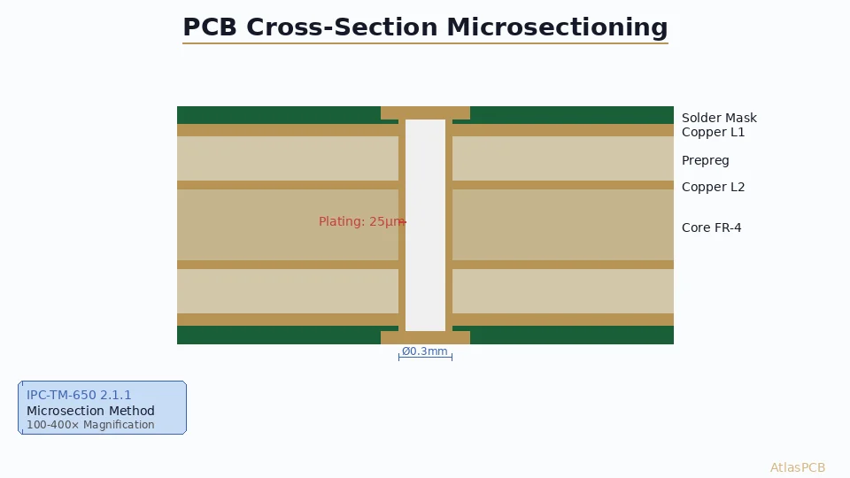
Cross-Section Microsectioning
Microsectioning remains the definitive method for plating void detection and is the basis for IPC-6012 acceptance criteria. The process involves:
- Coupon selection — Dedicated test coupons on the panel edge or sacrificial board locations
- Mounting — Epoxy encapsulation of the coupon
- Grinding/polishing — Sequential abrasive steps (120→240→400→600→1200 grit, then alumina polish) to expose the via cross-section at the target plane
- Etching — Brief micro-etch (ammonium persulfate or ferric chloride) to reveal grain structure
- Microscopy — Optical examination at 100–500× magnification
- Measurement — Plating thickness, void dimensions, and interconnect evaluation
IPC-6012 Acceptance Criteria:
| Parameter | Class 1 (General) | Class 2 (Dedicated) | Class 3 (High Reliability) |
|---|---|---|---|
| Minimum barrel thickness | 20 µm average | 20 µm average | 25 µm minimum |
| Voids per via | ≤3 not in same plane | ≤1 not reducing min thickness | None reducing min thickness |
| Interconnect defect | Wicking OK if no separation | ≤1 void per interconnect | No separation; full 360° bond |
| Etchback (if specified) | 13–80 µm | 13–80 µm | 13–80 µm |
Electrical Testing
Continuity testing (flying probe or bed-of-nails fixture) detects voids that cause complete opens but cannot identify partial voids that may propagate under thermal stress. The test applies a current (typically 100 mA) and measures resistance; any reading above the threshold (usually 10–50 Ω) flags a failure.
4-wire resistance measurement on daisy-chain test coupons provides higher sensitivity. By measuring the resistance of a chain of 20–100 vias in series, a single high-resistance void increases the chain resistance above the statistical control limit, even if the void doesn’t cause a complete open.
For a comparison of electrical test methods, see our article on [PCB electrical testing: flying probe vs fixture]/blog/pcb-electrical-testing-flying-probe-vs-fixture/).
Thermal Stress Testing
Solder float test: The test coupon is floated on 288°C molten solder for 10 seconds, then microsectioned. Thermal shock propagates any latent voids into visible cracks or separations. Per IPC-TM-650 Method 2.6.8, this is the standard qualification test for via plating integrity.
Interconnect Stress Test (IST): Passes current through via chains to cycle temperature between ambient and 150–200°C at 2–5 minute intervals. Resistance is monitored continuously; a 10% increase indicates void propagation. IST is more sensitive than solder float for detecting borderline voids.
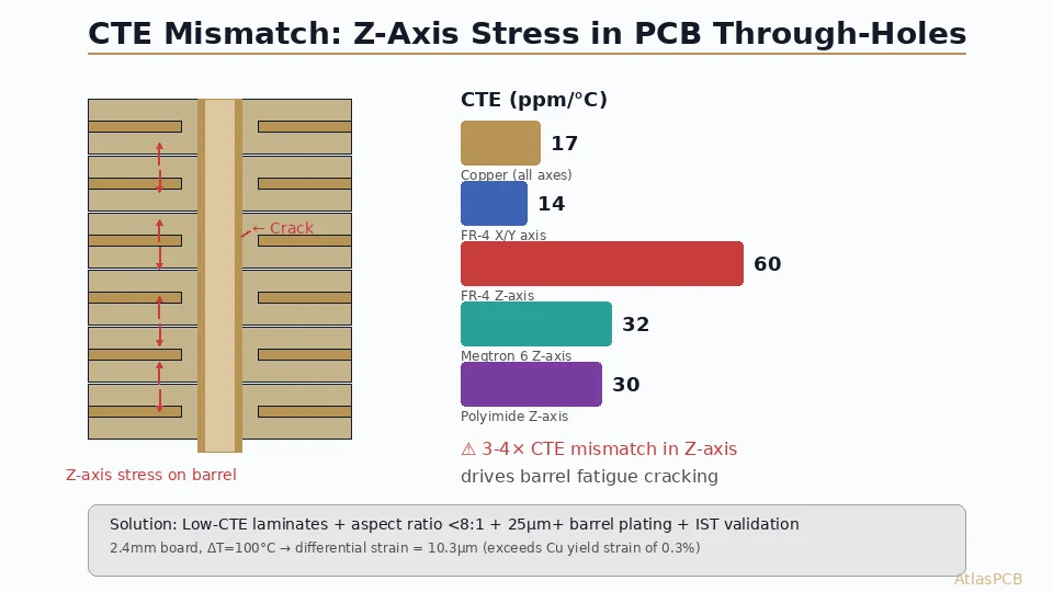
Thermal cycling: Extended cycling (-55°C to +125°C or -40°C to +125°C for automotive) per IPC-TM-650 Method 2.6.7.2 subjects vias to repeated CTE mismatch stress. Voids act as stress concentrators that propagate into barrel cracks over hundreds of cycles.
For more on reliability qualification methods, see our [PCB reliability testing]/blog/pcb-reliability-testing/) guide.
Advanced Detection Methods
X-ray micro-CT: Non-destructive 3D imaging of via interiors at 1–5 µm resolution. Can detect voids without destroying the sample, enabling 100% inspection of high-reliability assemblies. Equipment cost ($200K–$1M+) limits use to qualification and failure analysis.
Time-Domain Reflectometry (TDR): Sends a fast pulse through the via and analyzes reflections. Impedance discontinuities caused by voids create characteristic reflection signatures. Useful for detecting voids in buried vias that cannot be optically inspected.
Acoustic microscopy (C-SAM): Ultrasonic imaging can detect delamination and large voids at interfaces. Resolution is limited (~10 µm) but the method is non-destructive.
Process Control Strategy
Statistical Process Control (SPC)
Effective void prevention requires SPC monitoring at each critical process step:
| Process Step | Key Parameter | Measurement Frequency | Control Limit (Typical) |
|---|---|---|---|
| Drilling | Drill bit hit count | Each bit | ≤3,000 hits (FR-4) |
| Drilling | Hole wall roughness (Ra) | 1× per panel lot | ≤8 µm |
| Desmear | Permanganate concentration | 2× per shift | 55–65 g/L KMnO₄ |
| Desmear | Solution temperature | Continuous | 75–85°C ±2°C |
| Desmear | Etchback depth | 1× per lot | 5–15 µm target |
| Electroless Cu | Bath pH | 2× per shift | 12.3–12.8 |
| Electroless Cu | Copper concentration | 1× per shift | 2.5–3.5 g/L |
| Electroless Cu | Formaldehyde concentration | 2× per shift | 3.0–5.0 g/L |
| Electroless Cu | Deposition rate | 1× per shift (test panel) | 2.0–3.5 µm/hr |
| Electrolytic Cu | Current density | Continuous | 1.5–3.0 A/dm² (DC) |
| Electrolytic Cu | Bath temperature | Continuous | 22–28°C ±1°C |
| Electrolytic Cu | Organic additive levels | 1× per shift (CVS analysis) | Per supplier spec ±10% |
| Cross-section | Barrel plating thickness | 3× per lot minimum | ≥25 µm (Class 3) |
Desmear Process Optimization
The desmear process is the single highest-leverage point for void prevention. A robust desmear protocol includes:
Three-step alkaline permanganate process:
- Solvent swell (60–70°C, 5 min) — Organic solvent (butyl carbitol or equivalent) swells the resin surface, making it accessible to permanganate attack
- Permanganate etch (80°C, 10–12 min) — KMnO₄ at 55–65 g/L + NaOH at 40–50 g/L oxidizes and removes resin smear; manganese dioxide residue deposited on wall
- Neutralization/reduction (45°C, 5 min) — Acidic reducing agent (hydroxylamine sulfate or equivalent) dissolves MnO₂ residue, leaving a clean, micro-roughened surface for catalyst adhesion
Critical controls:
- Permanganate replenishment rate must match consumption (monitor by titration or ORP)
- Sodium hydroxide concentration affects selectivity — too high attacks glass fibers
- Rinse water quality between steps must meet <5 µS/cm conductivity to prevent drag-in contamination
- Solution aging — older solutions may have accumulated reaction byproducts reducing effectiveness; periodic dump-and-recharge on a scheduled cycle
Electroless Copper Optimization
Catalyst line critical controls:
- Conditioner: Uniform wetting verified by water-break test on test panels. Conditioner solution replaced on a fixed schedule (typically every 200–400 m² of panel throughput)
- Catalyst (Pd/Sn): Palladium concentration monitored by atomic absorption spectroscopy (target 150–250 ppm Pd). Tin-to-palladium ratio maintained at 10:1 to 15:1
- Accelerator: Removes excess tin from catalyst, exposing active palladium sites. Under-acceleration leaves too much tin (poor activity); over-acceleration strips palladium (skip-plating)
Electroless copper bath controls:
- Copper replenishment tied to panel throughput (4–6 g Cu²⁺ consumed per m² of plated area)
- Formaldehyde consumption monitored and replenished automatically or semi-automatically
- Bath loading (panel area per liter) controlled to prevent localized depletion: maximum 0.5 dm²/L
- Air agitation provides oxygen for the electroless reaction and maintains solution homogeneity
- Bath life monitoring — cumulative MTO (metal turnovers) tracked; bath replaced at 8–15 MTO depending on chemistry
Electrolytic Plating Optimization
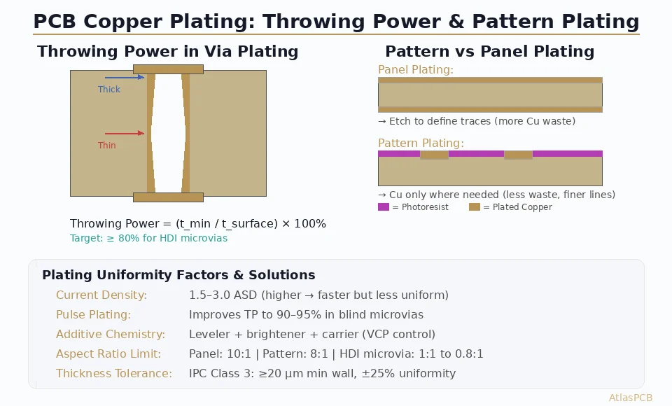
Throwing power — the ability of the plating bath to deposit copper uniformly from surface to mid-barrel — is the critical parameter for barrel void prevention during electrolytic plating.
Factors affecting throwing power:
| Factor | Effect on Throwing Power | Optimization |
|---|---|---|
| H₂SO₄ concentration | Higher acid → better TP | Maintain 60–80 g/L |
| CuSO₄ concentration | Lower copper → better TP | 200–220 g/L (don’t over-concentrate) |
| Current density | Lower CD → better TP | 1.5–2.5 A/dm² for high AR holes |
| Agitation | Better agitation → better TP | Eductor + oscillation + air |
| Leveler additive | Higher leveler → better TP | Per supplier recommendation |
| Temperature | Slightly higher → better TP | 24–26°C optimal |
| Pulse plating | Reverse pulse → much better TP | PPR: 15–25 ms forward, 1–3 ms reverse |
Pulse-reverse plating (PPR) is particularly effective for high-aspect-ratio holes. During the forward pulse, copper deposits preferentially at the hole opening (where current density is highest). During the brief reverse pulse, copper is selectively dissolved from the opening, thinning the deposit at the opening and improving uniformity. PPR can achieve >85% throwing power in 10:1 aspect ratio holes, compared to 55–70% for DC plating.
Case Studies in Void Prevention
Case Study 1: Automotive ECU — Interconnect Voids
Problem: A 6-layer FR-4 PCB for an engine control unit showed 4.2% via failure rate in IST testing, with cross-sections revealing interconnect voids at layer 3 and layer 4 connections.
Root Cause Analysis:
- Drill bits were used for 5,000 hits (specification: 3,000 maximum)
- Permanganate solution had drifted to 42 g/L (specification: 55–65 g/L)
- Desmear etchback measured at 2 µm (target: 5–15 µm)
Corrective Actions:
- Drill bit change interval reduced to 2,500 hits
- Permanganate concentration monitoring increased to every 4 hours
- Desmear time extended from 8 to 12 minutes
- Etchback target raised to 8–12 µm
Result: Via failure rate dropped to 0.05% in IST testing — below the 0.1% target for automotive Class 3 compliance.
Case Study 2: Server Backplane — Mid-Barrel Bubble Voids
Problem: A 24-layer, 3.2 mm thick backplane with 0.3 mm vias (aspect ratio 10.7:1) showed barrel voids in 2.8% of cross-sectioned vias, located consistently at mid-barrel.
Root Cause Analysis:
- Air bubbles trapped in high-aspect-ratio holes during immersion
- Eductor agitation insufficient for deep holes
- No panel oscillation in the plating tank
Corrective Actions:
- Added horizontal panel oscillation (2.5 m/min stroke)
- Pre-wetting step added: 60-second soak in dilute plating solution with ultrasonic agitation
- Initial current ramp: 50% current density for first 3 minutes, then full current
- Eductor flow velocity increased from 12 to 22 cm/s at board surface
Result: Barrel void incidence dropped from 2.8% to 0.15%, meeting the <0.5% internal quality target.
Case Study 3: HDI Smartphone Board — Microvia Voids
Problem: A 10-layer HDI board with 75 µm laser-drilled microvias showed random void defects after copper filling, visible as dimples on the via surface.
Root Cause Analysis:
- Electroless copper catalyst was insufficiently depositing in the blind via bottom
- Via aspect ratio (0.8:1) combined with small diameter limited solution exchange
- Organic residue from laser drilling not fully removed by desmear
Corrective Actions:
- Switched from permanganate to plasma desmear for laser-drilled microvias
- Extended catalyst immersion time from 3 to 6 minutes with megasonic agitation
- Electroless copper bath loading reduced from 0.6 to 0.35 dm²/L
- Added a second activation step (proprietary palladium activator)
Result: Microvia void rate reduced from 1.8% to 0.08%, meeting IPC-6012 Class 3 requirements for the smartphone OEM.
Design for Via Reliability
PCB designers can significantly reduce plating void risk through design choices:
Aspect Ratio Management
| Aspect Ratio | Void Risk | Recommended Approach |
|---|---|---|
| <6:1 | Low | Standard DC plating |
| 6:1 to 10:1 | Moderate | PPR plating, enhanced agitation |
| 10:1 to 15:1 | High | PPR plating, specialized process, wider tolerances |
| >15:1 | Very high | Consider sequential lamination to reduce AR |
Via Design Best Practices
- Minimum drill size: Avoid drilling below 0.15 mm mechanically; use laser drilling for smaller holes
- Pad annular ring: Maintain ≥75 µm annular ring for reliable interconnect formation
- Aspect ratio limit: Communicate with fabricator; typical maximum is 12:1 for Class 3 reliability
- Thermal relief: Use 4-spoke thermal reliefs on inner-layer power/ground connections to reduce drill smear from excessive heat sinking during drilling
- Via-in-pad: When using via-in-pad designs, specify [resin plug via process]/blog/pcb-resin-plug-via-process/) with cap plating to ensure void-free fill
- Stacked microvias: Limit stacked microvia depth to 3 levels; each additional level increases void risk at the bottom via
Communication with Your Fabricator
Specify the following in your fabrication notes to support void-free processing:
- IPC class requirement (Class 2 or Class 3) — this sets the acceptance criteria
- Minimum plating thickness — 25 µm for Class 3; specify if greater is needed
- Cross-section requirements — Number of coupons, locations, and reporting format
- IST or thermal stress qualification — If required for your application
- Material constraints — Specific laminate systems that may require adjusted desmear processing
Industry Standards Reference
| Standard | Scope | Relevance to Plating Voids |
|---|---|---|
| IPC-6012E | Qualification and Performance Specification for Rigid PCBs | Defines class-based acceptance criteria for plating thickness and voids |
| IPC-A-600K | Acceptability of Printed Boards | Visual reference for void classification and accept/reject decisions |
| IPC-TM-650 2.6.8 | Thermal Stress (Solder Float) | Test method for void detection via thermal shock |
| IPC-TM-650 2.1.1 | Microsectioning | Procedure for cross-section preparation and examination |
| IPC-9151 | IST Test Method | Procedure for interconnect stress testing |
| J-STD-003 | Solderability Tests | Evaluates surface condition that can indicate void-related issues |
Conclusion
Plating voids in PCB vias are a preventable defect when process fundamentals are understood and controlled. The three pillars of void prevention are:
- Thorough desmear — Ensure complete resin removal at all interconnect locations through properly maintained permanganate or plasma processes
- Continuous electroless copper — Maintain catalyst and electroless bath chemistry within specification to achieve uniform seed layer coverage
- Optimized electroplating — Control agitation, current density, and bath chemistry to prevent bubble entrapment and ensure adequate throwing power
Combined with statistical process control, regular cross-section monitoring, and design-for-manufacturability practices, these measures can reduce plating void rates below 0.1% — meeting the stringent requirements of automotive, aerospace, and high-reliability electronics applications.
Need confidence in your via reliability? Upload your Gerbers for a free engineering review — our process engineering team will evaluate your design for plating void risk and recommend optimized via structures for your reliability requirements.
Further Reading
- [Rogers PCB Fabrication: Material Sourcing, Lead Times & Quality Control]/blog/rogers-pcb-fabrication/)
- [PCB Rigid-Flex Bend Zone Reliability: Design Rules, Material Selection & Lifecycle Testing]/blog/pcb-rigid-flex-bend-zone-reliability/)
- [PCB Aspect Ratio: Via Depth-to-Diameter Rules and Manufacturing Limits]/blog/pcb-aspect-ratio-via-design/)
- [ENEPIG vs ENIG Surface Finish: Complete Comparison for Wire Bonding, Solderability, and Long-Term Reliability]/blog/enepig-vs-enig-surface-finish-wire-bonding/)
- [PCB Surface Finish Comparison: OSP vs HASL vs Immersion Silver vs ENIG for Assembly Reliability]/blog/pcb-surface-finish-osp-hasl-enig-immersion-silver-comparison/)
- Our Manufacturing Capabilities
About AtlasPCB — We specialize in complex PCB manufacturing for HDI, RF, and high-reliability applications. Explore our full PCB manufacturing capabilities, or get an instant online quote . Every order includes free engineering review. Get your quote.
Reviewed by AtlasPCB Engineering Team — IPC-certified manufacturing specialists with 15+ years of production experience in HDI, RF, and high-reliability PCB fabrication. Content based on factory floor data and real customer design reviews.
- plating-void
- via-reliability
- electroplating
- pcb-defects
- quality-control