· AtlasPCB Engineering · Engineering · 13 min read
Resin Plug Via Process: When, Why, and How to Specify Filled Vias
Everything PCB designers need to know about resin-filled vias — from IPC-4761 fill types and via-in-pad requirements to planarization specifications, copper capping, and cost implications. A practical guide to specifying filled vias correctly.
Resin Plug Via Process: When, Why, and How to Specify Filled Vias
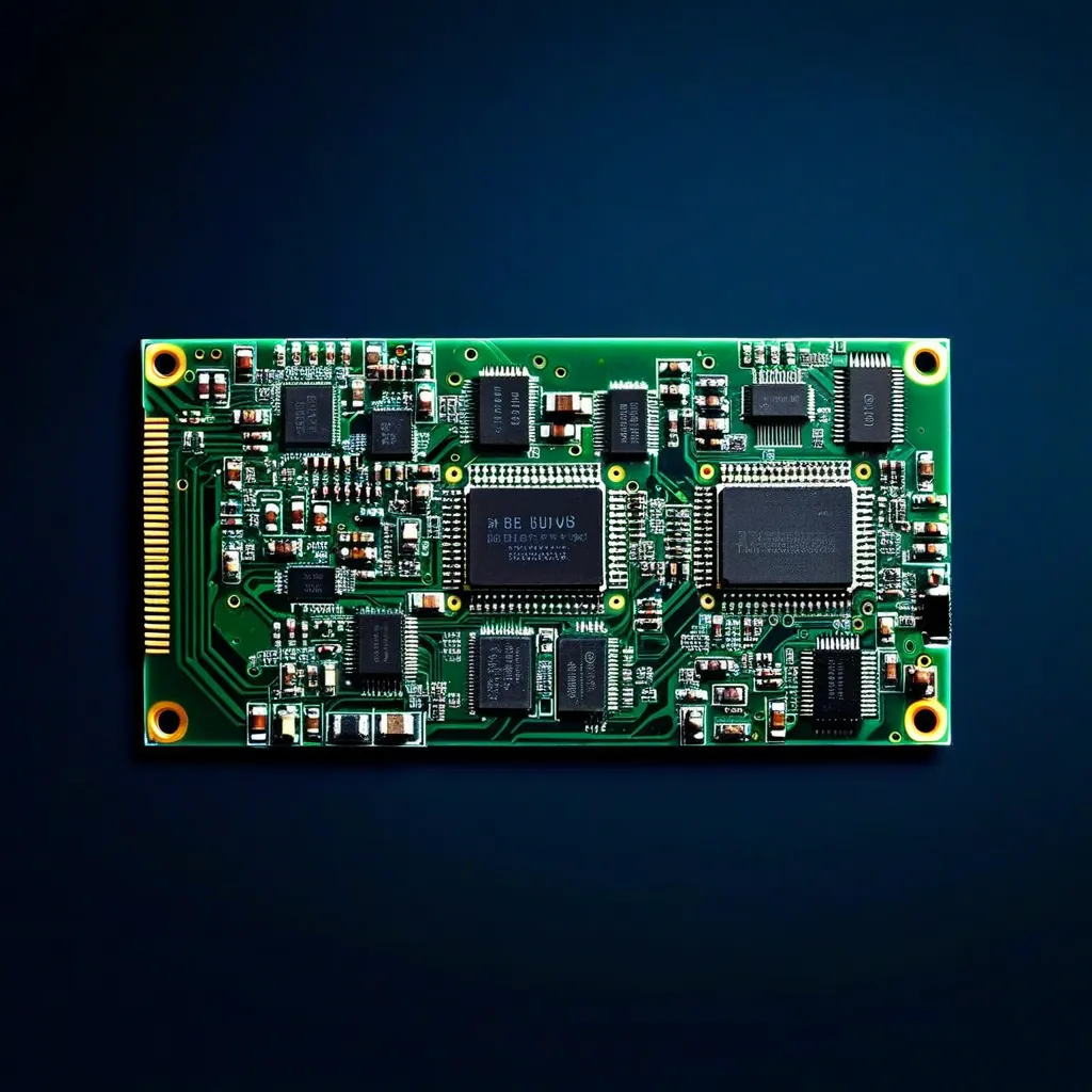
Open vias — holes plated with copper but left hollow inside — are perfectly adequate for most PCB designs. But as component pitch shrinks and board density increases, open vias create problems. An open via under a BGA pad wicks solder away from the joint during reflow, creating voids and unreliable connections. An open via between HDI buildup layers cannot support subsequent lamination without collapsing. An open via on a test pad catches probe tips and damages fixtures.
Resin-filled vias solve these problems by filling the hole with a non-conductive or conductive material, grinding the surface flat, and optionally capping with copper to create a fully functional pad. It’s a straightforward concept with significant process complexity and cost implications.
This guide covers when to specify filled vias, the IPC-4761 classification system, the physical filling process, planarization and capping requirements, design specifications you need to communicate to your fabricator, and the cost impact you should expect.
Why Fill Vias? The Engineering Case
Via-in-Pad for BGA Escape Routing
The most common reason for resin-filled vias is via-in-pad (VIP) design, where vias are placed directly in the component pad rather than being fanned out to the side. This technique is essential for:
Fine-pitch BGAs (≤0.8 mm pitch): There isn’t enough space between pads to fan out vias. A 0.5 mm pitch BGA with 0.25 mm pads leaves only 0.25 mm between pads — insufficient for a via pad, trace, and clearance. Placing the via directly in the BGA pad eliminates the fan-out entirely.
High pin-count BGAs: Large BGAs (>500 pins) with multiple rows of interior balls cannot escape all signals through the outer rows alone. Inner balls must route directly down through via-in-pad to inner layers.
Thermal pad connections: Many power components (MOSFETs, voltage regulators, power amplifiers) have exposed thermal pads on their underside. These pads require multiple vias to inner ground/power planes for thermal dissipation. Via-in-pad with resin fill allows solder attachment to the thermal pad without solder wicking into the vias.
Without resin fill, solder applied to a via-in-pad during reflow would flow into the open hole by capillary action, starving the solder joint above and creating voids in the BGA ball. For more on this topic, see our guide on [via-in-pad design]/blog/via-in-pad-design/).
Preventing Solder Wicking
Even vias not directly under component pads can cause solder wicking problems. A via in or near a soldering pad (within 0.3 mm) can wick solder away from the intended joint. This is particularly problematic with:
- Wave soldering: Molten solder is pushed through open vias by capillary action and wave pressure
- Selective soldering: Similar capillary effects in through-hole component vias
- Reflow of paste-in-hole components: Open vias near through-hole pins allow paste to escape
Filling these vias with resin eliminates the capillary pathway.
Sequential Lamination Requirements
In HDI designs using sequential lamination (buildup technology), buried vias on inner layers must be filled before the next lamination cycle. An unfilled buried via would collapse under lamination pressure, creating a dimple in the surface layers above and below — compromising copper thickness, impedance control, and structural integrity.
For detailed information on blind via fill technology in HDI designs, see our guide on [blind via fill technology]/blog/pcb-blind-via-fill-technology/).
Flat Surface Requirements
Some applications require absolutely flat via surfaces:
- Wire bonding: Bond wires cannot attach reliably to non-flat surfaces; filled and planarized vias provide the necessary flatness
- Probe testing: Flying probe or bed-of-nails test fixtures require consistent pad heights; dimpled vias cause probe misregistration or damage
- Flip-chip attachment: Controlled-collapse chip connection (C4) bumps require planar surfaces within ±15 µm
IPC-4761: Via Protection Classification
IPC-4761 “Design Guide for Protection of Printed Board Via Structures” defines seven types of via protection, ranging from simple coverage to fully filled and capped. Understanding this classification system is essential for clear communication with your fabricator.
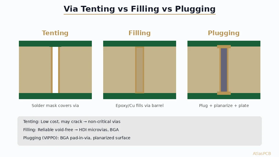
Type I: Tented Via
The simplest form — dry film soldermask covers the via opening on one or both sides. No fill material. The mask may or may not fully seal the via; IPC-4761 allows some mask recession into the hole. Suitable for non-critical vias that just need cosmetic coverage.
Limitations: Mask can crack or bubble over the unsupported span, especially for vias ≥0.4 mm diameter. Not suitable for via-in-pad.
Type II: Tented and Covered Via
Similar to Type I, but with additional liquid material (secondary mask or epoxy) applied to ensure the tent is sealed. Provides better hermeticity than Type I but still doesn’t fill the via interior.
Type III: Plugged Via
The via is partially filled from one side with a non-conductive material (soldermask, liquid epoxy, or paste). The plug may not fill the entire via depth — some void space is acceptable. This is a lower-cost alternative to full fill for applications that primarily need to prevent solder wicking.
Limitations: Surface may not be flat. Not suitable for component mounting pads.
Type IV: Plugged and Covered Via
Plugged from one side (Type III) with additional soldermask tenting on the opposite side. Provides solder wicking prevention from both board surfaces.
Type V: Filled Via
The via is completely filled with non-conductive material (resin) from both sides, with no remaining void space. The fill material extends to or slightly above the board surface. This is the first type suitable for structural applications (HDI buried vias).
Limitations: Fill surface may be slightly domed or recessed; not planarized.
Type VI: Filled and Planarized Via
Fully filled (Type V) with the fill material ground flat to the board surface. Provides a smooth, coplanar surface. Suitable for subsequent lamination in HDI processes. IPC-4761 specifies fill dimple/protrusion limits (typically ≤5 µm for Class 3).
Limitations: The exposed fill surface is non-conductive resin, not copper. Cannot directly receive solder.
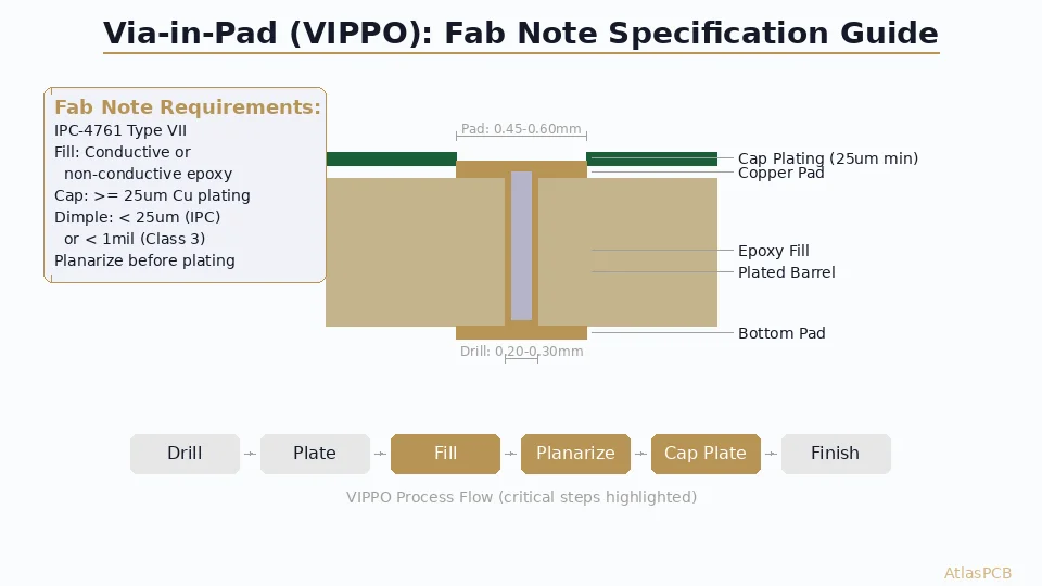
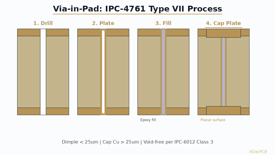
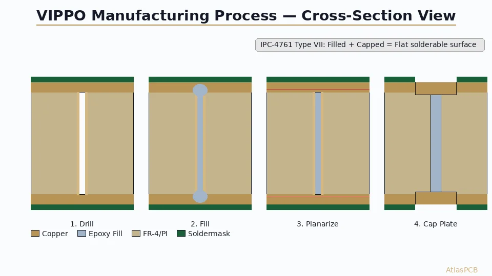
Type VII: Filled, Planarized, and Capped Via
The gold standard. Fully filled, planarized, then overplated with copper to create a conductive pad surface identical to a standard copper pad. This is what “via-in-pad with resin fill” means in practice. The component sees a flat copper pad; the fact that a via exists beneath it is invisible from a soldering perspective.
The Physical Filling Process
Step 1: Screen Printing or Vacuum Fill
The most common filling method uses a screen printing process, similar to solder paste printing but with resin instead of paste. A stencil with openings aligned to the via locations is placed over the panel, and resin is squeegeed through the openings into the holes.
For high-aspect-ratio vias or very small holes (<0.2 mm), vacuum-assisted filling provides more reliable void-free fill. The panel is placed in a vacuum chamber, resin is applied, and atmospheric pressure forces the resin into evacuated holes when vacuum is released.
Fill materials are typically two-component epoxy systems formulated for PCB via fill:
- Low CTE (typically 30–50 ppm/°C, matched to copper and FR4)
- Tg above reflow temperature (typically >150°C)
- Low shrinkage during cure (<1%)
- Good adhesion to copper barrel walls
- Compatible with subsequent plating chemistry (for Type VII)
Common via fill resins include products from Peters, San-Ei Kagaku (PHP-900 series), and Taiyo Ink.
Step 2: Curing
Filled panels are cured in a convection oven. Typical cure profiles:
- Stage 1: Ramp to 80°C, hold 30 minutes (drives off solvents)
- Stage 2: Ramp to 150°C, hold 60–120 minutes (cross-links epoxy)
Precise cure control is critical. Under-cured resin is soft, which causes problems during planarization (smearing, tearing). Over-cured resin becomes brittle, potentially cracking during thermal cycling.
Step 3: Planarization
After curing, the resin protrudes above the board surface. Ceramic or diamond abrasive belts grind the excess resin (and any copper overhang) flush with the board surface. This step requires:
- Precise thickness control: Removing too little leaves bumps; removing too much exposes uncured resin or thins the surface copper
- Flatness specification: IPC-4761 Type VI/VII requires fill surface within ±5 µm (0.2 mil) of the surrounding copper for Class 3
- No copper thinning: The grinding process must not reduce the surface copper below the minimum specified thickness
Step 4: Copper Capping (Type VII Only)
For Type VII vias, the planarized surface receives an additional copper plating cycle:
- Surface preparation: Micro-etch and clean the planarized surface to ensure adhesion between the resin fill and the new copper layer
- Electroless copper: Deposit a thin seed layer over the resin surface (since resin is non-conductive)
- Electrolytic copper: Build up copper to the specified thickness (typically 15–25 µm)
- The result: A continuous copper pad that spans the original copper annular ring and the filled via center, creating a solderable surface indistinguishable from a solid copper pad
The copper cap adhesion to the underlying resin is a critical quality factor. Poor adhesion causes cap lifting during thermal cycling, which manifests as pad cratering during assembly. IPC-6012 Class 3 requires the cap to survive 6× solder float at 288°C without separation.
Resin Fill vs Copper Fill
While resin (non-conductive) fill is by far the most common, conductive copper fill is an alternative for applications requiring electrical conductivity through the via fill material:
Resin Fill (Non-Conductive)
- Material: Epoxy-based paste, typically loaded with silica or ceramic filler for CTE matching
- Cost: Lower — simpler process, no additional plating
- Electrical: Non-conductive through the fill; current flows only through the copper barrel
- Thermal: Moderate thermal conductivity (0.5–2 W/m·K) — adequate for most applications
- Use case: Via-in-pad, HDI buried via fill, solder wicking prevention — the vast majority of applications
Copper Fill (Conductive)
- Material: Electrolytic copper deposited by specialized plating processes
- Cost: Significantly higher — requires extended plating time and specialized bath chemistry
- Electrical: Fully conductive through the entire via cross-section — lower resistance than barrel-only
- Thermal: Excellent thermal conductivity (385 W/m·K) — ideal for thermal vias
- Use case: High-current applications, thermal management, aerospace/military requirements
For most commercial and industrial designs, resin fill with copper cap (Type VII) is the correct choice. The copper barrel provides adequate electrical conductivity, and the resin fill provides the structural and surface flatness benefits at lower cost.
Specifying Filled Vias in Your Design
Clear specifications prevent misunderstandings and re-spins. Here’s what to include in your fabrication documentation:
Fab Drawing Callouts
NOTES:
1. Via-in-pad vias (identified in drill chart as "VIP") shall be filled
   per IPC-4761 Type VII: non-conductive epoxy fill, planarized, and
   copper capped.
2. Fill dimple/protrusion: ±5 µm maximum (IPC-6012 Class 3).
3. Copper cap thickness: 15 µm minimum.
4. All other vias may remain open (standard plated through-hole).
Design Data Requirements
In your Gerber/IPC-2581 data, clearly differentiate which vias require filling:
- Separate drill files for filled vias and open vias
- Clear drill chart marking which hole sizes/symbols require fill
- Callout in fab notes cross-referencing drill symbols
Common Specification Mistakes
Mistake 1: Specifying fill on all vias. Unless every via needs fill, specify only the ones that require it. Filling all vias can increase cost by 30–50% unnecessarily.
Mistake 2: Not specifying fill type. “Fill vias with resin” is ambiguous. Specify the IPC-4761 type (most commonly Type VII for via-in-pad applications). Include whether planarization and copper capping are required.
Mistake 3: Incorrect annular ring calculation. The via-in-pad annular ring must be calculated from the finished (plated) hole, not the drilled hole. A 0.30 mm drilled hole with 25 µm plating has a 0.25 mm finished hole. If the pad diameter is 0.55 mm, the annular ring is (0.55 − 0.25) / 2 = 0.15 mm — tight but feasible for most fabricators.
Mistake 4: Via size too large for reliable fill. Resin fill works reliably for vias up to about 0.6 mm diameter (for through-holes in 1.6 mm boards). Larger vias may require multiple fill-and-cure cycles or alternative fill methods, significantly increasing cost and process time.
Cost Impact Analysis
Resin plug via processing is not free. Understanding the cost drivers helps you specify it only where needed:
| Cost Driver | Impact |
|---|---|
| Base fill process (setup, materials) | +10–15% of base board cost |
| Planarization | +3–5% additional |
| Copper capping (additional plating cycle) | +5–10% additional |
| Total for Type VII (fill + planarize + cap) | +15–30% of base board cost |
Volume sensitivity: The per-unit cost decreases with volume because setup costs (stencil fabrication, process qualification) are amortized. For a 100-piece prototype order, resin fill might add 25–30%. For a 10,000-piece production order, the adder drops to 15–20%.
Via count sensitivity: Boards with only 10–20 filled vias cost nearly the same as boards with 200 filled vias (the process runs on the entire panel regardless). The main variable is whether additional stencils or fill operations are needed for different hole sizes.
Cost Optimization Strategies
- Minimize the number of different filled via sizes. Each unique hole size may require a separate fill stencil.
- Use via-in-pad only where necessary. Fan-out vias to dog-bone pads where space permits; reserve via-in-pad for fine-pitch BGAs where fan-out isn’t possible.
- Consider Type V or VI where Type VII isn’t needed. If the filled via isn’t a component pad, you may not need the copper cap, saving an entire plating cycle.
- Group filled vias on one board side when possible. Single-sided fill is cheaper than double-sided fill.
For [BGA escape routing]/blog/bga-escape-routing/) strategies that minimize the need for via-in-pad, refer to our routing guide.
Reliability Considerations
Thermal Cycling Performance
The CTE mismatch between the resin fill material (30–50 ppm/°C) and the surrounding copper barrel (17 ppm/°C) creates stress during thermal cycling. Well-formulated fill resins are designed to accommodate this mismatch through controlled compliance, but extreme thermal cycling (-55°C to +125°C, thousands of cycles) can eventually cause:
- Resin shrinkage and separation from the barrel wall
- Copper cap cracking or delamination
- Fill material degradation above Tg
For high-reliability applications (automotive, aerospace), specify fill resins with Tg ≥ 170°C and verify thermal cycling performance with IST (Interconnect Stress Testing) or accelerated thermal cycling per IPC-TM-650.
Moisture Sensitivity
Cured epoxy fill materials absorb moisture (typically 0.3–0.8% by weight). Absorbed moisture can volatilize during reflow, creating internal pressure that may crack the resin or delaminate the copper cap. Proper baking before assembly (4 hours at 125°C per IPC-1601) mitigates this risk, particularly for boards stored in uncontrolled environments.
Electrical Considerations
Non-conductive resin fill does not affect the via’s electrical performance — current flows through the copper barrel exactly as it does in an open via. However, the resin does change the via’s thermal behavior: a resin-filled via dissipates heat slightly less effectively than an open via (which benefits from convective cooling through the hole) but slightly more effectively than a solid copper-filled via would suggest, because the resin-copper interface provides additional surface area for conduction.
For thermal management applications requiring maximum heat transfer, copper-filled vias or arrays of open thermal vias may be more appropriate than resin-filled ones.
Conclusion
Resin-filled vias are an essential technique for modern high-density PCB designs. Whether you’re routing escape vias under a 0.4 mm pitch BGA, preventing solder wicking on a complex mixed-technology assembly, or building HDI stackups with sequential lamination, understanding the fill process and specifying it correctly ensures manufacturing success.
The key principles are straightforward: specify the IPC-4761 type that matches your functional requirement (Type VII for via-in-pad, Type V/VI for structural fill), clearly identify which vias need fill in your fabrication data, keep via sizes within process-friendly ranges (≤0.6 mm for reliable single-pass fill), and budget for the 15–30% cost adder that this additional processing requires.
When your design pushes the boundaries — very high aspect ratios, extremely fine pitch, or demanding reliability requirements — engage your fabricator’s engineering team early. A collaborative approach to via fill specification prevents surprises at both the manufacturing and assembly stages.
Ready to start your project? Upload your Gerbers for a free engineering review, or talk to an engineer about your design requirements.
Further Reading
- [BGA Pad Design and Via-in-Pad: How to Prevent Solder Voiding in High Pin-Count BGA Assemblies]/blog/bga-pad-design-via-in-pad-solder-voiding-prevention/)
- [Via-in-Pad Design: Filled, Capped, and Plated Over — Complete Guide]/blog/via-in-pad-design/)
- [PCB Thermal Management: Heat Dissipation Techniques for Reliable Electronics]/blog/pcb-thermal-management/)
- [Press-Fit Via Design for PCB Connectors: Hole Sizing, Plating & IPC Compliance]/blog/pcb-press-fit-via-design/)
- [PCB Copper Plating Process: Electroless vs Electrolytic Copper for HDI Vias and High-Density Interconnects]/blog/pcb-copper-plating-electroless-vs-electrolytic-hdi-vias/)
- HDI PCB Manufacturing
About AtlasPCB — We specialize in complex PCB manufacturing for HDI, RF, and high-reliability applications. Explore our HDI PCB manufacturing capabilities, or get an full PCB manufacturing capabilities . Every order includes free engineering review. Get your quote.
Reviewed by AtlasPCB Engineering Team — IPC-certified manufacturing specialists with 15+ years of production experience in HDI, RF, and high-reliability PCB fabrication. Content based on factory floor data and real customer design reviews.
- resin-plug
- via-fill
- ipc-4761
- via-in-pad
- bga-design