· AtlasPCB Engineering · Engineering · 10 min read
PCB Drilling Aspect Ratio Limits: Mechanical vs Laser Drill Capabilities
Understand PCB drill aspect ratio limits for mechanical and laser drilling. Learn how hole diameter, board thickness, and drill technology affect via reliability and manufacturability.
Introduction to PCB Drill Aspect Ratio
The aspect ratio of a drilled hole in a PCB — defined as the ratio of board thickness to the finished hole diameter — is one of the most critical manufacturability parameters in circuit board design. It directly determines whether a plated through-hole (PTH) or via can be reliably fabricated with adequate copper coverage throughout the barrel.
As PCB designs push toward higher layer counts, finer pitches, and increased density, understanding the practical limits of both mechanical and laser drilling becomes essential. Designers who ignore aspect ratio constraints risk costly redesigns, yield losses, and — worst of all — latent reliability failures that surface only in the field.
This guide provides practical aspect ratio limits for both mechanical and laser drilling, explains the physics behind these limits, and offers actionable design guidelines to keep your boards manufacturable. For a broader overview of via design parameters, see our [via size selection guide]/blog/pcb-via-size-selection-guide/).
Defining Aspect Ratio in PCB Drilling
The Basic Formula
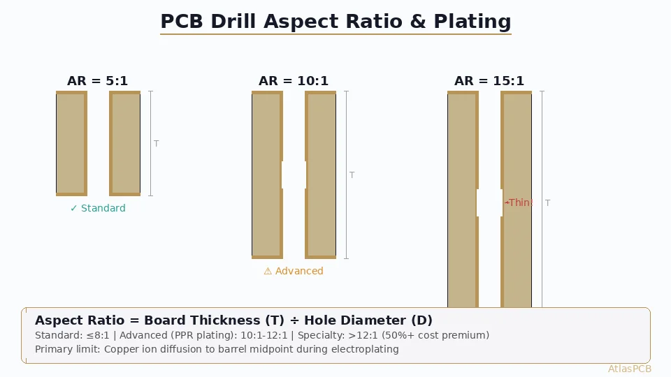
Aspect Ratio = Board Thickness ÷ Drilled Hole Diameter
For a 1.6 mm thick board with a 0.3 mm drill:
- Aspect ratio = 1.6 / 0.3 = 5.3:1
Important clarifications:
- Use the drilled (pre-plating) hole diameter, not the finished hole diameter
- Board thickness means the total laminate thickness at the drill location
- For blind vias, use the depth of the via rather than total board thickness
Why Aspect Ratio Matters
The aspect ratio directly affects the electroplating process. During copper electroplating, the electrolyte must flow into the hole and deposit copper uniformly along the entire barrel length. As the aspect ratio increases:
- Electrolyte exchange at the center of the barrel becomes increasingly difficult
- Current density distribution becomes non-uniform, with higher deposition at the hole entry
- Throwing power of the plating bath is challenged, creating thinner copper at the midpoint
- Gas bubbles can become trapped, causing voids
IPC-6012 specifies minimum copper plating thickness requirements: 20 µm average with 18 µm minimum for Class 2, and 25 µm average with 20 µm minimum for Class 3. Meeting these minimums at the barrel midpoint becomes the primary challenge at high aspect ratios.
Mechanical Drilling Aspect Ratio Limits
Standard Production Capabilities
| Aspect Ratio | Typical Min Drill Size | Application | Yield Impact |
|---|---|---|---|
| <6:1 | 0.25 mm+ | Standard production | Minimal — routine process |
| 6:1 – 8:1 | 0.20 mm+ | Advanced standard | Low — well-controlled process |
| 8:1 – 10:1 | 0.15 mm+ | High-density | Moderate — requires process optimization |
| 10:1 – 12:1 | 0.15 mm+ | Advanced HDI | Significant — specialized equipment needed |
| 12:1 – 15:1 | 0.15 mm+ | Extreme applications | High — expect yield reduction and premium pricing |
| >15:1 | Special | Backplane/thick boards | Very high — few fabricators capable |
The 10:1 Rule of Thumb
The widely cited 10:1 aspect ratio limit represents the practical boundary where standard PCB fabrication processes can reliably produce plated holes. Beyond 10:1:
- Plating chemistry requires advanced high-throw formulations
- Drill bit management becomes critical (more frequent replacement, reduced stack height)
- Deburring and desmear processes need optimization for deep holes
- Inspection requires more extensive cross-sectioning
For [IPC Class 3 high-reliability designs]/blog/ipc-class-3-requirements/), many fabricators recommend staying at 8:1 or below to provide additional manufacturing margin.
Mechanical Drill Bit Limitations
The aspect ratio is not just about plating — the drill bit itself has physical constraints:
Minimum practical drill sizes by board thickness:
| Board Thickness | Min Recommended Drill | Resulting Aspect Ratio |
|---|---|---|
| 0.8 mm | 0.15 mm (6 mil) | 5.3:1 |
| 1.0 mm | 0.15 mm (6 mil) | 6.7:1 |
| 1.6 mm | 0.20 mm (8 mil) | 8.0:1 |
| 2.0 mm | 0.25 mm (10 mil) | 8.0:1 |
| 2.4 mm | 0.25 mm (10 mil) | 9.6:1 |
| 3.2 mm | 0.35 mm (14 mil) | 9.1:1 |
Drill bit deflection is a key concern. Smaller drill bits are more flexible and prone to:
- Wandering (positional accuracy degrades)
- Breakage (especially in high-Tg or filled materials)
- Reduced hit count before replacement
Standard carbide micro-drills in the 0.15–0.20 mm range typically achieve 1,000–3,000 hits before replacement, compared to 5,000+ hits for 0.30 mm drills. This directly impacts production cost.
Strategies for High Aspect Ratio Mechanical Drilling
When designs require aspect ratios approaching or exceeding 10:1, several strategies can help:
- Controlled-depth drilling — Drill from both sides to meet in the middle (requires precise depth control)
- Step drilling — Use a pilot drill followed by a finishing drill
- Reduced stack height — Drill fewer panels simultaneously for better accuracy
- Specialized drill bits — Use under-cut or parabolic flute designs for better chip evacuation
- Optimized drill parameters — Lower spindle speeds (80,000–100,000 RPM vs standard 150,000+ RPM), adjusted feed rates, and pecking cycles
For more on how aspect ratio affects via design decisions, refer to our [aspect ratio via design guide]/blog/pcb-aspect-ratio-via-design/).
Laser Drilling Aspect Ratio Limits
UV Laser Drilling (Nd:YAG / UV-DPSS)
UV lasers (typically 355 nm wavelength) are the workhorse for microvia drilling in HDI PCBs. Their aspect ratio capabilities:
| Parameter | Standard Process | Advanced Process |
|---|---|---|
| Typical hole diameter | 75–150 µm | 50–75 µm |
| Minimum hole diameter | 50 µm | 25–30 µm |
| Maximum depth per layer | 80–100 µm | 60–80 µm |
| Aspect ratio (standard) | 0.75:1 | 0.8:1 |
| Aspect ratio (maximum) | 1:1 | 1.2:1 |
UV lasers can ablate both copper and dielectric, making them suitable for conformal mask drilling where the laser penetrates the copper capture pad and the underlying dielectric in a single process.
CO2 Laser Drilling
CO2 lasers (9.4 or 10.6 µm wavelength) cannot directly ablate copper, so they require a window opening in the top copper layer (either by etching or UV laser pre-drill). Their characteristics:
| Parameter | Standard Process | Advanced Process |
|---|---|---|
| Typical hole diameter | 100–200 µm | 75–125 µm |
| Minimum hole diameter | 75 µm | 60 µm |
| Maximum depth per layer | 100–120 µm | 80–100 µm |
| Aspect ratio (standard) | 0.75:1 | 1:1 |
| Aspect ratio (maximum) | 1:1 | 1.5:1 |
CO2 lasers are faster than UV lasers (processing speed of 1,000–3,000 holes per second vs 200–500 for UV) but produce larger holes with more taper.
Why Laser Via Aspect Ratios Are Lower
The physics of laser drilling fundamentally limits the achievable aspect ratio compared to mechanical drilling:
- Beam divergence — As the laser penetrates deeper, the beam expands, creating a tapered hole profile
- Plasma shielding — Ablated material creates a plasma that absorbs subsequent laser pulses
- Debris redeposition — Ablated copper and resin can deposit on the hole walls, reducing effective diameter
- Bottom clearance — The laser must fully expose the target pad at the bottom for reliable interconnection
A typical microvia cross-section shows a top diameter 10–20% larger than the bottom diameter. This taper is normal and must be accounted for in the design rules.
Stacked and Staggered Microvias
To achieve connectivity across multiple layers using laser-drilled microvias, designers use stacked or staggered configurations:
- Stacked microvias: Drilled directly on top of each other (requires via fill and planarization between layers)
- Staggered microvias: Offset from each other on alternating layers (less demanding but uses more routing area)
For stacked microvias spanning 3+ layers, the effective aspect ratio of the total interconnect structure becomes a reliability concern, even though each individual via meets its aspect ratio limit. IPC-2226 provides guidance on stacked microvia reliability. For an in-depth discussion of HDI via structures, see our [HDI PCB design guide]/blog/hdi-pcb-design-guide/).
Aspect Ratio Impact on Plating Quality
The Midpoint Plating Problem
The most critical plating quality metric for high-aspect-ratio holes is the copper thickness at the barrel midpoint relative to the surface copper thickness. This ratio is called the throwing power of the plating process.
For an ideal process:
- Throwing power = 100% (uniform plating throughout)
In practice:
- Aspect ratio 5:1 → ~80–90% throwing power (standard chemistry)
- Aspect ratio 8:1 → ~65–75% throwing power
- Aspect ratio 10:1 → ~50–65% throwing power
- Aspect ratio 12:1 → ~40–55% throwing power
Advanced plating chemistries (PPR — Periodic Pulse Reverse plating) can significantly improve throwing power at high aspect ratios, achieving 70–80% at 10:1.
Failure Modes at Excessive Aspect Ratios
Barrel cracking: Insufficient copper at the midpoint creates a weak point that cracks during thermal excursions. The Z-axis expansion of the laminate creates tensile stress on the barrel, and thin copper cannot withstand repeated cycling.
Corner cracking (knee cracking): The transition point where the barrel meets the surface pad is a stress concentration. High aspect ratios exacerbate this because the plating distribution is poorest in this region.
Void formation: Air bubbles or plating solution decomposition products trapped in deep holes create voids in the copper. These voids act as crack initiation sites and increase electrical resistance.
Wedge voids: Specific to via-in-pad designs where the via is filled after plating. Incomplete fill creates a wedge-shaped void at the barrel midpoint. Learn more about [via-in-pad design considerations]/blog/via-in-pad-design/).
Design Guidelines by Application
Standard Commercial Products (IPC Class 2)
- Target aspect ratio: ≤8:1
- Minimum mechanical drill: 0.20 mm (8 mil)
- Minimum laser via: 100 µm
- This covers the vast majority of consumer and industrial electronics
High-Reliability / Aerospace (IPC Class 3)
- Target aspect ratio: ≤8:1 (preferred), 10:1 maximum
- Minimum mechanical drill: 0.25 mm (10 mil)
- Minimum laser via: 100 µm
- Require IST (Interconnect Stress Testing) qualification for aspect ratios >8:1
- See our [IPC Class 3 requirements guide]/blog/ipc-class-3-requirements/) for full specification details
HDI / Mobile Devices
- Microvia aspect ratio: ≤1:1 per layer
- Stacked microvias: Maximum 3 levels without additional reliability testing
- Minimum via diameter: 75 µm (production), 50 µm (advanced)
- Via fill required for stacked configurations
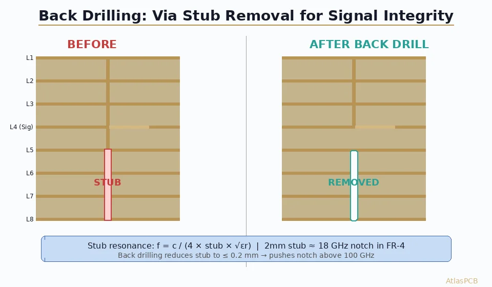
Backplane / Thick Board Designs
- Board thickness may reach 4–6 mm or more
- Aspect ratios of 10:1–15:1 may be unavoidable
- Consider back-drilling to remove unused barrel stubs for signal integrity
- Use via-in-pad with back-drill rather than through-hole vias where possible
- Sequential lamination with buried vias can reduce the maximum aspect ratio required
Practical Design Checklist
Before finalizing your drill table, verify the following:
- Calculate aspect ratios for every unique drill size against the total board thickness
- Flag any via with an aspect ratio exceeding 8:1 — confirm with your fabricator
- Specify drill class in fabrication notes (e.g., “Maximum aspect ratio 10:1”)
- Consider via-in-pad for BGA fanout to avoid aspect ratio issues with dog-bone vias on inner layers
- Check annular ring requirements — high aspect ratios demand tighter drill registration, which eats into annular ring margin. See our [annular ring standards guide]/blog/pcb-annular-ring-ipc-standards/)
- Run DFM check — automated tools can flag aspect ratio violations. Our [DFM checklist]/blog/pcb-dfm-checklist/) covers this and other critical parameters
- Consult your fabricator early for designs with aspect ratios >10:1
Comparing Mechanical and Laser Drilling: Summary
| Parameter | Mechanical Drill | UV Laser | CO2 Laser |
|---|---|---|---|
| Hole diameter range | 0.15–6.5 mm | 25–150 µm | 60–200 µm |
| Maximum aspect ratio | 10:1 (standard) | 1:1 (standard) | 1:1 (standard) |
| Through-hole capable | Yes | No (blind only) | No (blind only) |
| Copper penetration | Yes | Yes | No (window required) |
| Speed (holes/sec) | 3–5 | 200–500 | 1,000–3,000 |
| Position accuracy | ±25 µm | ±10 µm | ±15 µm |
| Hole wall quality | Smooth (with desmear) | Good (some resin smear) | Moderate (more taper) |
| Cost driver | Drill bit wear | Laser maintenance | Laser maintenance |
Emerging Technologies
Direct Laser Drilling of Through-Holes
Some advanced fabricators are experimenting with high-power UV lasers to drill through-holes in thin boards (<0.8 mm). While not yet mainstream, this eliminates drill bit wear and achieves better positional accuracy than mechanical drilling for very small holes (<0.10 mm).
Plasma Drilling
Plasma-based drilling using focused ion beams or atmospheric plasma jets is being researched for ultra-high-aspect-ratio holes. Current laboratory results show aspect ratios of 20:1+ in thin substrates, but the technology is years away from production viability.
Improved Plating Chemistry
The development of next-generation high-throwing-power plating chemistries continues to push the practical aspect ratio boundary upward. Modern PPR plating with advanced brightener/leveler systems can achieve reliable plating at 15:1 aspect ratios in controlled production environments.
Conclusion
Understanding PCB drill aspect ratio limits is essential for producing manufacturable, reliable circuit boards. The key takeaways:
- Mechanical drilling: Target ≤8:1 for standard production, ≤10:1 for advanced, and consult your fabricator for anything beyond
- Laser drilling: Keep microvias at ≤1:1 aspect ratio per dielectric layer
- Plating quality degrades progressively with increasing aspect ratio — there is no hard cutoff, but rather increasing risk
- Early fabricator engagement is critical for any design pushing aspect ratio boundaries
- Design alternatives like HDI stackups with microvias, sequential lamination, and buried vias can often eliminate the need for extreme aspect ratios
For a comprehensive view of the [PCB manufacturing process]/blog/pcb-manufacturing-process-15-steps/) and how drilling fits into the overall flow, visit our manufacturing guide. Atlas PCB engineers are available to review your drill table and recommend optimizations.
Atlas PCB specializes in high-aspect-ratio drilling and HDI fabrication with advanced laser and mechanical drilling capabilities. Contact us for engineering support and a free DFM review on your next project.
Further Reading
- [Rogers PCB Fabrication: Material Sourcing, Lead Times & Quality Control]/blog/rogers-pcb-fabrication/)
- [PCB Manufacturer with Engineering Review: Why Human DFM Audit Matters]/blog/pcb-manufacturer-engineering-review/)
- [ENEPIG vs ENIG: Which PCB Surface Finish for Your Design?]/blog/enepig-vs-enig/)
- [PCB Surface Finish Selection — ENIG vs HASL vs OSP vs Hard Gold vs ENEPIG]/blog/pcb-surface-finish-enig-hasl-osp-hard-gold-enepig/)
- [Medical PCB Manufacturing: FDA Compliance, Traceability & Reliability]/blog/medical-pcb-manufacturing-requirements/)
- Our Manufacturing Capabilities
About AtlasPCB — We specialize in complex PCB manufacturing for HDI, RF, and high-reliability applications. Explore our full PCB manufacturing capabilities, or get an instant online quote . Every order includes free engineering review. Get your quote.
Reviewed by AtlasPCB Engineering Team — IPC-certified manufacturing specialists with 15+ years of production experience in HDI, RF, and high-reliability PCB fabrication. Content based on factory floor data and real customer design reviews.
- drilling
- aspect-ratio
- mechanical-drill
- laser-drill