· AtlasPCB Engineering · Engineering · 12 min read
PCB Dielectric Constant (Dk) Measurement: Methods, Accuracy & Impact on Impedance Control
Understand PCB dielectric constant measurement methods, accuracy factors, and how Dk variations affect impedance control in high-frequency circuit board design.

Why Dielectric Constant Matters in PCB Design
The dielectric constant (Dk, also called relative permittivity or εr) of a PCB laminate is one of the most fundamental material properties in circuit board design. It directly determines two critical electrical characteristics:
Signal propagation speed — signals travel through a dielectric medium at a speed inversely proportional to √Dk. Higher Dk means slower propagation and longer electrical delay per unit length.
Characteristic impedance — the impedance of a transmission line is inversely proportional to √Dk (for stripline) or √Dk_eff (for microstrip). A higher Dk results in lower impedance for the same trace geometry.
For digital designers working with [high-speed signals]/blog/high-speed-pcb-design/), Dk accuracy determines whether impedance targets are met. For RF engineers designing [high-frequency circuits]/blog/rf-pcb-design-guidelines/), Dk stability across frequency and temperature determines circuit performance. In both cases, understanding how Dk is measured — and how much the measurement can be trusted — is essential engineering knowledge.
The Physics of Dielectric Constant
What Dk Actually Represents
The dielectric constant quantifies how much a material concentrates electric flux compared to vacuum. A material with Dk = 4.0 stores four times the electric energy per unit volume as the same geometry in free space.
This energy storage occurs through polarization — the alignment of molecular dipoles and displacement of electron clouds in response to an applied electric field. In PCB laminates, multiple polarization mechanisms contribute:
- Electronic polarization — displacement of electron clouds around atoms. Very fast, active at all frequencies through the optical range.
- Atomic/ionic polarization — displacement of atoms within molecules. Active through the infrared region.
- Dipolar (orientational) polarization — rotation of polar molecules. This is the slowest mechanism and the primary reason Dk decreases with frequency in polymer-based laminates.
Frequency Dependence
Because dipolar polarization cannot follow rapid field oscillations, the Dk of PCB laminates decreases with increasing frequency. This is not a defect — it is fundamental physics.
For a typical FR-4 laminate:
- Dk at 1 MHz: approximately 4.5–4.7
- Dk at 1 GHz: approximately 4.2–4.4
- Dk at 10 GHz: approximately 3.9–4.1
This 10–15% variation across frequency has significant implications for impedance calculation. Using a 1 MHz Dk value (as often published in basic datasheets) for a 10 GHz design will produce impedance errors of 5–8%.
Low-loss laminates designed for [high-speed applications]/blog/pcb-high-speed-material-dk-df-comparison/) generally show less Dk variation with frequency because they use resin systems with fewer polar molecular groups.
Temperature and Moisture Effects
Dk also varies with temperature and moisture content:
- Temperature: Dk typically increases by 0.01–0.03 per °C for FR-4 type laminates. This means a board operating at 85°C may have a Dk that is 1–2% higher than at 25°C.
- Moisture absorption: Water has a Dk of approximately 80. Even small amounts of absorbed moisture significantly increase the effective Dk of a laminate. A laminate that absorbs 0.3% moisture by weight may see Dk increase by 2–4%.
These effects are particularly important for designs that must maintain [controlled impedance]/blog/controlled-impedance-pcb/) across environmental conditions.
Measurement Methods
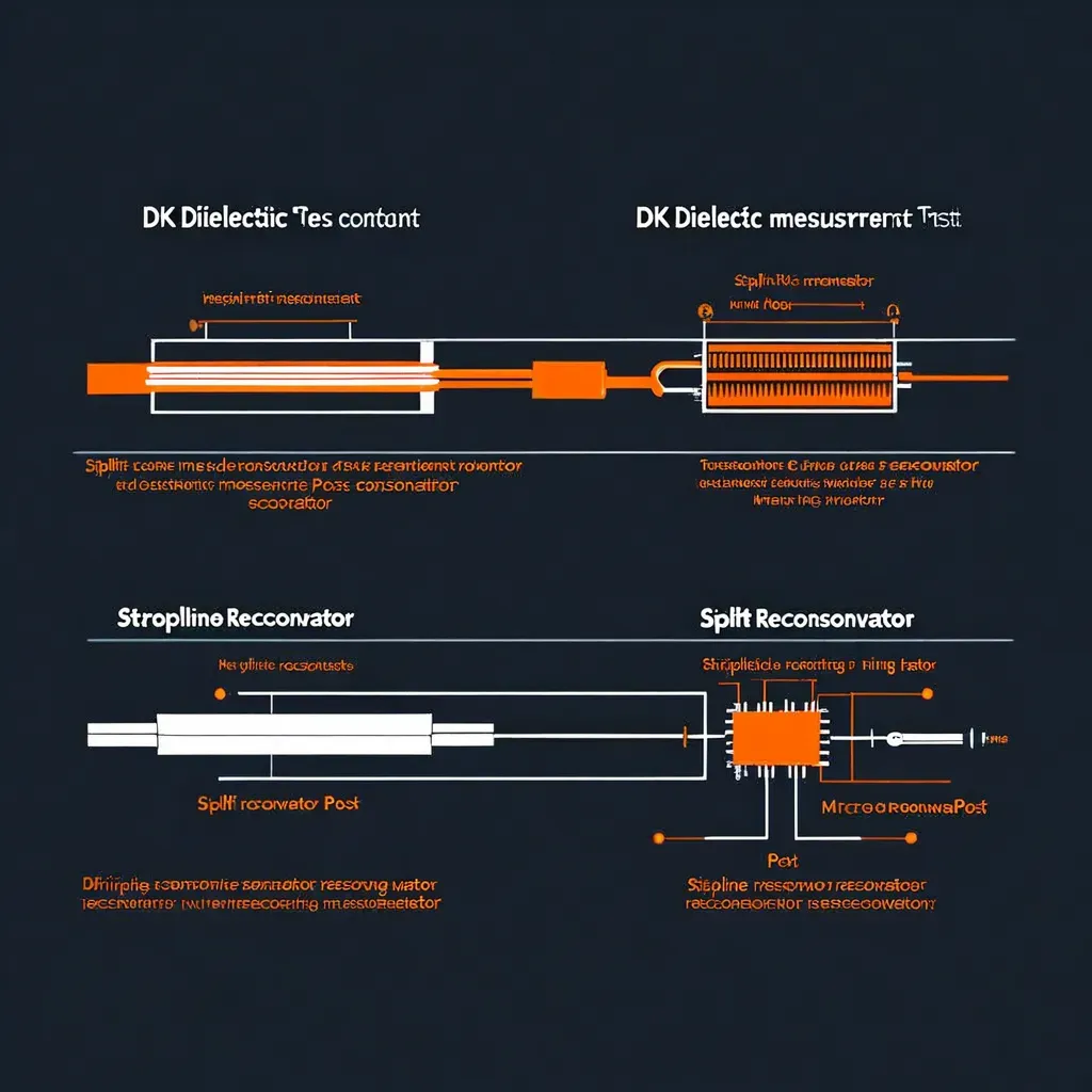
IPC-TM-650 Stripline Resonator (Method 2.5.5.5)
The IPC stripline resonator method is the most widely used technique in the PCB industry and forms the basis for most published Dk values on laminate datasheets.
How it works:
A stripline resonator is fabricated by etching a precisely dimensioned conductor between two ground planes using the laminate under test as the dielectric. The resonator is excited through loosely coupled probes, and the resonant frequencies are measured using a vector network analyzer (VNA).
The Dk is calculated from:
Dk = (n × c)² ÷ (2 × L × f_n)²
Where:
- n = resonance mode number
- c = speed of light in vacuum
- L = resonator length
- f_n = measured resonant frequency of mode n
Advantages:
- Directly measures Dk in a configuration representative of actual PCB use (stripline)
- Well-documented, standardized procedure
- Provides Dk at multiple discrete frequencies (from the multiple resonance modes)
- Accounts for copper roughness effects implicitly
Limitations:
- Requires fabrication of a test coupon — adds cost and lead time
- Measurement accuracy depends on coupon fabrication quality
- Provides Dk only at discrete frequencies corresponding to resonance modes
- The result is an “effective Dk” that includes copper roughness effects, not the intrinsic material Dk
Typical accuracy: ±2–3% for well-fabricated coupons
Split-Post Dielectric Resonator (SPDR)
The SPDR method measures a flat sheet of material placed between two precisely machined dielectric resonator halves.
How it works:
A dielectric resonator (typically sapphire or barium titanate) is split into two halves. The laminate sample is inserted in the gap between the halves. The resonator’s resonant frequency shifts in proportion to the Dk of the inserted sample, and the quality factor changes in proportion to the dissipation factor (Df).
Advantages:
- Non-destructive — the sample does not need to be processed or etched
- Fast measurement — results in minutes rather than weeks
- Good accuracy for thin samples
- Single-frequency measurement is very precise
Limitations:
- Measures at a single frequency (determined by the resonator design)
- Does not account for copper roughness effects
- Sample must be flat and uniform in thickness
- The measured Dk is the intrinsic material property, which differs from the effective Dk seen by traces on a PCB
Typical accuracy: ±1% at the measurement frequency
Full-Sheet Resonance (FSR)
FSR uses a copper-clad laminate panel itself as a parallel-plate resonator.
How it works:
A copper-clad laminate sheet with known dimensions is placed in a fixture that capacitively couples to the panel edges. The panel resonates at frequencies determined by its dimensions and the Dk of the laminate. By measuring multiple resonant modes, Dk can be determined across a range of frequencies.
Advantages:
- Measures production material directly — no special coupon fabrication needed
- Provides Dk at multiple frequencies from a single measurement
- Can measure large sample areas, averaging out local variations
- Good for incoming material quality verification
Limitations:
- Requires uniform copper cladding — cannot measure processed boards
- Edge effects and copper conductivity affect accuracy
- Less precise than SPDR for absolute Dk values
- Panel dimensions must be accurately known
Typical accuracy: ±2–4%
Transmission Line Methods
Several transmission line methods extract Dk from measurements on fabricated PCB structures:
Time-Domain Reflectometry (TDR): A fast-rise-time pulse is sent down a known-length transmission line, and the propagation delay is measured. Dk is calculated from the delay:
Dk_eff = (t_d × c ÷ L)²
Where t_d is the one-way propagation delay, c is the speed of light, and L is the trace length.
TDR provides the effective Dk that includes all real-world effects (copper roughness, solder mask, glass weave). This makes it valuable for verifying that impedance will match the design intent.
Differential Phase Length: Two transmission lines of different lengths but identical cross-section are measured with a VNA. The phase difference between them yields propagation velocity and hence Dk. This method cancels out connector and launch effects, improving accuracy.
Typical accuracy: ±2–5% depending on technique and calibration quality
Sources of Dk Variation in Production
Resin Content Variation
PCB laminates are composite materials consisting of woven glass fabric impregnated with resin. The Dk of glass fiber (approximately 6.2 for E-glass) is significantly different from the Dk of epoxy resin (approximately 3.0–3.5). Therefore, the ratio of glass to resin in the finished laminate directly affects the bulk Dk.
Resin content in production laminates typically varies ±2–3% from the nominal specification. This produces Dk variations of:
- E-glass with standard epoxy: approximately ±0.08 Dk per 1% resin content change
- NE-glass alternatives: approximately ±0.04 Dk per 1% change (because glass and resin Dk values are closer)
For a laminate with nominal Dk = 4.0, a ±3% resin content variation produces a Dk range of 3.76–4.24 — a spread that can push [impedance]/blog/pcb-impedance-control/) outside a ±5% tolerance window.
Glass Style Effects
Different glass weave styles have different glass-to-resin ratios and fiber bundle density:
| Glass Style | Thickness (mil) | Resin Content | Dk Range (10 GHz) |
|---|---|---|---|
| 106 | 1.5 | 70–75% | 3.5–3.7 |
| 1080 | 2.8 | 62–68% | 3.7–3.9 |
| 2116 | 3.7 | 50–55% | 3.9–4.1 |
| 7628 | 7.0 | 42–48% | 4.1–4.4 |
Designs that specify the glass style can reduce Dk uncertainty. For critical impedance applications, specifying spread-glass versions further reduces local Dk variation caused by the fiber weave pattern.
Lamination Process Influence
The lamination cycle affects final Dk through:
- Resin flow — excessive flow during lamination pushes resin away from high-pressure areas (under dense copper features), changing local resin content
- Cure degree — under-cured resin has a higher Dk than fully cured resin due to residual polar groups
- Void content — trapped air or volatiles create low-Dk voids that reduce effective Dk
These process variations add another ±1–2% to the Dk uncertainty in production boards.
Impact on Impedance Control
Impedance Sensitivity to Dk
The characteristic impedance of a transmission line depends on Dk through the following relationships:
Stripline (simplified): Z₀ ∝ 1 / √Dk
Microstrip (simplified): Z₀ ∝ 1 / √Dk_eff, where Dk_eff ≈ (Dk + 1)/2 + (Dk - 1)/2 × F(w/h)
A sensitivity analysis shows:
| Dk Change | Impedance Change (Stripline) | Impedance Change (Microstrip) |
|---|---|---|
| ±1% | ∓0.5% | ∓0.35% |
| ±3% | ∓1.5% | ∓1.05% |
| ±5% | ∓2.5% | ∓1.75% |
| ±10% | ∓5.0% | ∓3.5% |
For a 50 Ω stripline target with ±10% tolerance (45–55 Ω), a Dk error of up to ±20% could theoretically be tolerated from Dk alone. But in practice, Dk is only one of several variables (along with trace width, dielectric thickness, and copper thickness) that contribute to impedance variation. The total error budget must account for all sources simultaneously.
For high-speed designs requiring ±5% impedance tolerance, each contributing factor gets a tighter allocation. A practical Dk tolerance of ±3% is typically needed, which requires:
- Frequency-specific Dk data (not just 1 MHz values)
- Glass style specification to reduce weave effects
- Lot-specific material data for critical builds
For the detailed relationship between material properties and impedance, refer to our [impedance matching guide]/blog/pcb-impedance-matching-differential-pairs/).
Effective Dk vs. Bulk Dk in Design Calculations
A common source of impedance error is using the wrong Dk value in field solver calculations:
- Bulk (intrinsic) Dk — the material property measured by SPDR or material supplier testing. Does not include copper roughness, solder mask, or geometric effects.
- Effective (design) Dk — the apparent permittivity experienced by a signal on the actual PCB. Includes copper roughness (which increases apparent Dk by 2–8%), solder mask coating, and field fringing effects.
For stripline calculations, the difference between bulk and effective Dk is primarily due to copper roughness, adding 2–5% to the apparent Dk.
For [microstrip calculations]/blog/microstrip-vs-stripline/), the difference is larger because the electric field partially travels through air (Dk = 1.0) and partially through solder mask (Dk ≈ 3.2–3.8), making the effective Dk significantly lower than the bulk Dk of the core laminate.
Practical Dk Selection for Impedance Calculation
For reliable impedance calculation:
- Use frequency-appropriate Dk values — obtain Dk at the signal’s fundamental frequency or Nyquist frequency, not at 1 MHz
- Account for copper roughness — add 2–5% to the laminate Dk for stripline, or use a field solver that models roughness explicitly
- Include solder mask in microstrip models — specify solder mask Dk and thickness as separate layers
- Use the manufacturer’s validated Dk — request the specific Dk value your PCB manufacturer uses in their impedance modeling for the selected laminate. This “process Dk” incorporates their experience with actual fabrication outcomes.
- Verify with test coupons — for critical designs, request TDR measurement of impedance coupons on the production panel
Dk Measurement in Incoming Material Inspection
Why Incoming Inspection Matters
For high-reliability and high-frequency applications, measuring Dk of incoming laminate lots provides:
- Verification that the material meets the specification
- Lot-specific data for accurate impedance calculation
- Trend monitoring to detect supplier process drift
- Documentation for traceability in regulated industries
Practical Measurement Setup
For PCB fabricators performing incoming Dk inspection:
SPDR measurement at 10 GHz provides a rapid, non-destructive screening tool. Compare results to the supplier’s datasheet value with an acceptance window of ±3%.
Clad resonator (FSR) measurement on copper-clad panels provides Dk at multiple frequencies and reflects the actual copper-clad material that will be processed.
Process coupons fabricated alongside production boards provide the most relevant data — the effective Dk after all processing steps.
The ideal approach combines SPDR for incoming verification with process coupon measurement for impedance model refinement.
Material Selection Based on Dk Requirements
Matching Dk to Design Needs
Different applications require different Dk properties:
High-speed digital (PCIe, DDR, Ethernet):
- Moderate Dk (3.3–4.0) at the signal frequency
- Low Dk variation with frequency (flat Dk profile)
- Tight Dk tolerance lot-to-lot
- See our [material selection guide]/blog/pcb-material-selection-guide/) for recommended laminates
RF and microwave:
- Dk matched to the circuit design (often 3.0–3.5 for RF PCBs)
- Very low Dk variation with temperature (especially for filters and oscillators)
- Tight Dk tolerance within a single panel (for antenna arrays)
- Stable Dk with moisture absorption
Mixed-signal:
- Dk compatible with both digital impedance requirements and analog circuit tuning
- Consider different materials for different board regions in [hybrid stackups]/blog/pcb-stackup-design-guide/)
Dk and Stackup Optimization
When the available Dk values do not exactly match the design requirement, the stackup geometry can be adjusted to compensate:
- Higher Dk than needed → increase dielectric thickness or reduce trace width to maintain impedance
- Lower Dk than needed → decrease dielectric thickness or increase trace width
This flexibility is limited by manufacturing capability. Trace widths below 3 mil and dielectric thicknesses below 3 mil push into HDI territory with associated cost implications.
A [stackup calculator]/blog/pcb-stackup-calculator/) that incorporates frequency-dependent Dk data is essential for this optimization.
Emerging Trends in Dk Measurement
Broadband Characterization
Modern high-speed designs require Dk data across a broad frequency range (DC to 50+ GHz). New measurement techniques are emerging:
- Differential characterization using precision test fixtures and de-embedding algorithms provides continuous Dk and Df data from 100 MHz to 50 GHz
- On-board measurement structures embedded in production PCBs allow real-time Dk verification
- Machine learning correlation between SPDR point measurements and broadband behavior reduces the need for expensive wideband testing
Digital Twin Material Models
Advanced signal integrity simulators now support frequency-dependent material models (Djordjevic-Sarkar, Wideband Debye) that capture the full Dk(f) curve from a few measured data points. Providing accurate anchor points at 1, 10, and 40 GHz enables these models to interpolate and extrapolate with ±1% accuracy across the full frequency range.
Conclusion
Dielectric constant measurement is not an academic exercise — it directly determines whether your PCB meets impedance specifications and electrical performance targets. The gap between datasheet Dk values and actual production Dk can easily be 5–10%, which translates to 2.5–5% impedance error before any other manufacturing variables are considered.
The practical path to Dk accuracy:
- Start with frequency-specific datasheet values — never use 1 MHz data for GHz designs
- Specify glass style and resin content range to narrow production Dk variation
- Request lot-specific Dk data from your material supplier for critical builds
- Validate with TDR coupon measurements on production panels
- Close the loop — compare predicted and measured impedance to refine your Dk model over time
Need precise impedance control for your next design?
Upload your Gerbers for a free engineering review — our materials team will verify Dk assumptions, recommend the optimal laminate, and ensure your impedance targets are achievable in production. Get a quote today →
Further Reading
- [PCB Design for GaN and SiC Power Devices: Thermal Management, Layout Rules, and Material Selection]/blog/pcb-design-gan-sic-power-devices-thermal-layout/)
- [PCB Panelization and Array Design: V-Score vs Tab Routing, DFM Rules, and Cost Optimization]/blog/pcb-panelization-v-score-tab-routing-dfm-cost-optimization/)
- [mmWave PCB Material Selection: Rogers vs Megtron vs LCP for 5G and 6G Applications]/blog/mmwave-pcb-material-selection-rogers-megtron-lcp-5g-6g/)
- [Rogers PCB Fabrication: Material Sourcing, Lead Times & Quality Control]/blog/rogers-pcb-fabrication/)
- [PCB Rigid-Flex Bend Zone Reliability: Design Rules, Material Selection & Lifecycle Testing]/blog/pcb-rigid-flex-bend-zone-reliability/)
- Rigid PCB Manufacturing
About AtlasPCB — We specialize in complex PCB manufacturing for HDI, RF, and high-reliability applications. Explore our impedance-controlled PCB manufacturing . Every order includes free engineering review. Get your quote.
Reviewed by AtlasPCB Engineering Team — IPC-certified manufacturing specialists with 15+ years of production experience in HDI, RF, and high-reliability PCB fabrication. Content based on factory floor data and real customer design reviews.
- dielectric-constant
- dk
- materials
- impedance
- measurement