· AtlasPCB Engineering · Engineering · 8 min read
Asymmetric PCB Stackups: When Breaking Symmetry Improves High-Speed Performance
Learn when and why asymmetric PCB stackups outperform symmetric designs in high-speed, RF-digital hybrid, and thermal management applications — with practical layer assignment strategies and warpage mitigation techniques.
The Symmetry Paradigm — And Its Limits
Every PCB stackup design guide begins with the same rule: “Design your stackup symmetrically about the center.” This advice exists for excellent reasons — symmetric laminations naturally resist warpage, simplify impedance calculations, and ensure predictable manufacturing behavior.
But design rules exist to serve the product, not the other way around. When system-level requirements conflict with symmetric constraints, engineers face a choice: compromise performance to maintain symmetry, or intentionally break symmetry to achieve optimal electrical/thermal results.
This article explores when asymmetric stackups provide genuine advantages, how to manage their manufacturing challenges, and practical implementation strategies used in production designs.
When Symmetry Constrains Performance
Scenario 1: RF-Digital Hybrid Boards
A 5G small-cell radio with an integrated baseband processor needs:
- Top layers (L1–L2): 28 GHz antenna feeds on Rogers RO4350B (εr = 3.48, Df = 0.0037, 0.254 mm core)
- Inner layers (L3–L8): DDR4 routing, power planes, and FPGA I/O on standard Megtron 4 (εr = 3.8, Df = 0.005)
- Bottom layers (L9–L10): Power amplifier bias networks
A symmetric design would require Rogers material on both the top and bottom of the stack — doubling the expensive PTFE material cost even though the bottom layers carry only DC bias and low-frequency control signals.
An asymmetric approach places Rogers only where needed (top), uses low-cost FR-4 for the bottom half, and saves 35% in material cost while maintaining identical RF performance.
Scenario 2: Thermal Ground Plane Placement
In power electronics or high-power LED drivers, the primary heat-generating components mount on one surface. Optimal thermal performance requires a continuous ground/thermal plane as close to that surface as possible — ideally 0.1–0.2 mm below the component pads.
A symmetric 8-layer stackup might place the first ground plane at L2 with 0.2 mm spacing, but the opposing side would also need 0.2 mm to the bottom ground — even though no thermal load exists there. An asymmetric design can use 0.1 mm prepreg for L1→L2 (thermal path) and 0.3 mm for the bottom equivalent (L7→L8), reducing thermal resistance by 50% where it matters.
Scenario 3: BGA Escape Routing
Large BGAs (> 1500 balls) with 0.8 mm or 0.65 mm pitch require very thin dielectrics between routing layers to maintain impedance with narrow traces. The escape routing layers need 50–75 μm dielectric, but inner routing layers carrying bus signals at wider pitch can use standard 100–150 μm spacing.
A fully symmetric stackup would apply thin dielectric throughout, increasing layer count or forcing unnecessary constraints on non-critical layers.
Anatomy of a Well-Designed Asymmetric Stackup
An optimized asymmetric stackup follows these principles:
1. Identify the Performance-Critical Half
Determine which half of the board has tighter electrical requirements. Place the performance-critical layers in the “premium” half:
- RF signal layers → top half (if antenna/connector access is on top)
- High-speed differential pairs → closer to the reference plane that offers better impedance control
- Thermal planes → closest to heat sources
2. Match Glass Style Across the Midplane
The single most important warpage control mechanism is matching glass reinforcement style between corresponding layers above and below the center:
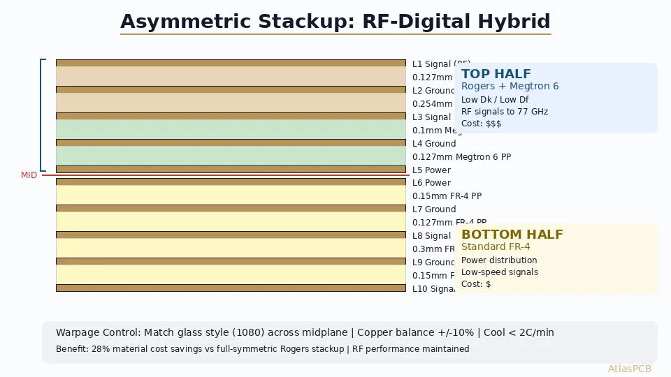
Layer Assignment Example (10-layer asymmetric):

L1  — Signal (RF)         | 0.127 mm 1080 prepreg (68% resin)
L2  — Ground              |
    — 0.254 mm 3313 core  |    TOP HALF
L3  — Signal (High-speed) |    (Rogers + low-Dk prepreg)
    — 0.1 mm 1080 prepreg |
L4  — Ground              |
    — 0.127 mm 1080 PP    |
L5  — Power               |
═══════ MIDPLANE ══════════
L6  — Power               |
    — 0.15 mm 1080 prepreg |
L7  — Ground              |    BOTTOM HALF
    — 0.127 mm 1080 PP    |    (Standard FR-4)
L8  — Signal              |
    — 0.3 mm 2116 core    |
L9  — Ground              |
    — 0.15 mm 2116 prepreg |
L10 — Signal/Power        |
Note: glass styles 1080 and 2116 have different X/Y CTE characteristics. Ideally, each prepreg layer above the midplane is mirrored by the same glass style below.
3. Compensate with Copper Balance
Copper density affects local CTE because copper’s CTE (~17 ppm/°C) differs from cured resin (~60 ppm/°C Z-axis). Asymmetric copper distribution creates differential shrinkage during cooling.
Solution: Add copper fill (ground pour or hatched copper at 50–70% coverage) on layers with lower component/trace density to equalize copper weight above and below the midplane within ±10%.
4. Select Compensating Resin Content
Higher resin content = higher CTE in the Z-axis but more compliant in X/Y. If the top half uses thinner dielectrics (less total resin), the bottom half should use prepregs with higher resin content to partially compensate the CTE imbalance:
- Top half total resin volume: 45%
- Bottom half target: 50–55% (slightly higher to offset the thinner prepregs above)
ATLAS PCB — ADVANCED STACKUP ENGINEERING
Custom Stackup Design & Impedance Modeling
Our engineering team designs optimized stackups for RF-digital hybrids, high-thermal applications, and complex HDI — including asymmetric configurations with warpage simulation. Free DFM review included.
Get Stackup Consultation →Warpage Prediction and Mitigation
Understanding the Physics
During lamination, the PCB stackup is heated to 180–200°C (above Tg) where resin is liquid and stress-free. Upon cooling, each layer contracts according to its CTE. In a symmetric stackup, contraction forces balance across the midplane → flat board.
In an asymmetric stackup, differential contraction creates a bending moment:
Warpage curvature κ ∝ Σ(E_i × t_i × α_i × ΔT × z_i) / Σ(E_i × t_i × z_i²)Where E is modulus, t is thickness, α is CTE, ΔT is the temperature change, and z is distance from neutral axis.
Simulation Approach
Before committing to an asymmetric stackup in production:
- Model the stackup in a thermo-mechanical FEA tool (Ansys Mechanical, MSC Nastran, or Moldex3D for resin flow + warpage)
- Include copper patterns — real copper distributions from the Gerber data affect local stiffness
- Simulate the cooling profile — faster cooling = more stress = more warpage
- Predict warpage — compare against IPC-6012 limits (0.75% for Class 3)
- Iterate — adjust dielectric thicknesses, resin content, or glass styles until warpage meets spec
Practical Warpage Limits
| Board Size | Class 2 Limit (1.5%) | Class 3 Limit (0.75%) |
|---|---|---|
| 100 × 100 mm | 1.5 mm | 0.75 mm |
| 200 × 150 mm | 3.0 mm | 1.5 mm |
| 300 × 250 mm | 4.5 mm (impractical) | 2.25 mm |
For large boards (> 200 mm), even small CTE imbalances produce significant warpage. Asymmetric stackups on large panels require more aggressive compensation.
Case Study: 16-Layer Radar/Comms Hybrid
A defense customer required a 16-layer board combining:
- 77 GHz automotive radar front-end (2 RF layers on Rogers RO3003)
- Digital signal processor (DDR4-3200, 4 routing layers on Megtron 6)
- Power management (3 power planes on standard FR-4)
Symmetric approach (rejected): Would require Rogers material on layers 15–16 (not needed), or repositioning RF layers to the center (unacceptable for antenna proximity). Total material cost: $340/board.
Asymmetric solution (implemented):
- Layers 1–4: Rogers RO3003 core + Megtron 6 prepreg (RF section)
- Layers 5–12: Megtron 6 cores/prepregs (digital section)
- Layers 13–16: Standard Tg170 FR-4 (power distribution)
Warpage management:
- 1080 glass style used for all prepregs (top and bottom)
- Ground pour on L15–L16 increased copper density to match top-half average
- Controlled cooling at 1.5°C/min below 150°C
- Final measured warpage: 0.42% (within Class 3 limit)
- Material cost: $245/board (28% savings)
RF-Digital Interface Considerations
When asymmetric stackups combine different dielectric materials, the interface between material regions requires attention:
Impedance Discontinuities
A trace transitioning from Rogers (εr = 3.48) to FR-4 (εr = 4.2) changes impedance unless trace width adjusts. Pre-calculate the width transition and implement a tapered width change over 3–5× the dielectric thickness.
Lamination Compatibility
Not all material combinations co-laminate well. Rogers RO4000 series is designed for FR-4 compatibility (same press cycle). Pure PTFE (RO3003) requires bonding films or specialized prepregs (like Arlon CuClad bondply) that add cost and complexity.
Thermal Expansion Mismatch at Material Boundaries
Different Z-axis CTE between Rogers and FR-4 creates interlaminar stress at the material boundary. Mitigation: place the material transition at a plane (ground/power) layer where there’s no signal-carrying trace crossing the boundary.
Design Guidelines for Asymmetric Stackups
- Document the asymmetry rationale — include a “stackup design intent” note in fabrication documentation explaining why symmetry was broken and what warpage mitigation is specified
- Specify glass style matching — call out required glass styles per layer in the stackup drawing (don’t leave it to the fabricator’s discretion)
- Add warpage spec to drawing — explicitly state maximum bow/twist tighter than IPC default if needed for your assembly process (typical SMT requires < 0.5% for large BGA boards)
- Include copper balance requirements — specify minimum copper coverage (%) for fill layers
- Require first-article warpage measurement — measure all 3 axes and provide a warpage map before production release
- Consider panelization effects — asymmetric boards may warp differently in different panel orientations; specify or constrain panel layout
When NOT to Use Asymmetric Stackups
Asymmetric designs add cost through:
- Extended engineering time (warpage simulation)
- Additional first-article verification
- Potentially lower panel yield (warpage rejects)
- Material handling complexity (multiple dielectric types)
Stay symmetric when:
- The board is small (< 80 mm) — warpage is naturally minimal
- Standard materials meet all impedance targets
- Volume is high and cost sensitivity is extreme
- Assembly uses wave soldering (warpage tolerance is very tight)
- You lack FEA simulation capability to predict warpage
Further Reading
- [PCB Stackup Symmetry and Balanced Lamination for Warpage Control]/blog/pcb-stackup-symmetry-balanced-lamination-warpage/)
- [PCB Hybrid Stackup: Combining Rogers and FR-4 for RF-Digital Designs]/blog/pcb-hybrid-stackup-rogers-fr4/)
- [Controlled Impedance PCB Design: Stackup Calculations]/blog/controlled-impedance-pcb-design-stackup-calculations/)
- [HDI PCB Stackup Design: Advanced Techniques]/blog/hdi-pcb-stackup-design-advanced/)
Planning an asymmetric stackup for your next design? AtlasPCB’s engineering team runs warpage simulation and impedance modeling as part of our standard DFM review — no extra charge. Start your project →
About AtlasPCB — We specialize in complex PCB manufacturing for HDI, RF, and high-reliability applications. Explore our RF and high-frequency PCB services, multilayer PCB fabrication up to 30 layers, or get an aluminum and metal-core PCB services . Every order includes free engineering review. Get your quote.
Reviewed by AtlasPCB Engineering Team — IPC-certified manufacturing specialists with 15+ years of production experience in HDI, RF, and high-reliability PCB fabrication. Content based on factory floor data and real customer design reviews.
- pcb stackup
- asymmetric lamination
- high speed design
- signal integrity
- warpage control
- rf digital hybrid
- thermal management
- layer assignment