· AtlasPCB Engineering · Engineering · 7 min read
Copper Balancing and Thieving for PCB: Preventing Warpage in Multilayer Boards
Learn how copper balancing and thieving patterns prevent bow and twist in multilayer PCBs. Covers design rules, IPC-2221 guidelines, DFM copper distribution, and practical CAD implementation for 4-layer to 20+ layer stackups.

Why Copper Distribution Matters for PCB Flatness
Every multilayer PCB undergoes thermal cycling during lamination (180°C for standard FR-4, up to 230°C for high-Tg materials) and reflow soldering (peak 250°C for SAC305). During these thermal events, copper and dielectric expand at vastly different rates — copper’s CTE is approximately 17 ppm/°C while FR-4 measures 14-18 ppm/°C in-plane. When one layer contains 90% copper coverage and its mirror layer only has 20%, the resulting stress differential induces permanent deformation.
This deformation manifests as bow (cylindrical curvature) and twist (corner-to-corner warpage), which causes several downstream problems:
- SMT assembly failure: Components tombstone, bridging, or open joints when the board surface deviates more than 0.75% of diagonal length
- BGA reliability issues: Solder balls crack under cyclic stress from residual warpage
- Panel utilization loss: Warped panels cannot be processed through automated assembly lines
- Connector mating problems: Edge connectors won’t seat properly in backplane slots
The solution lies in copper balancing — a DFM discipline that manages copper density distribution across all layers to minimize thermomechanical asymmetry.
Understanding Copper Density and Symmetry Rules
Layer Pair Symmetry
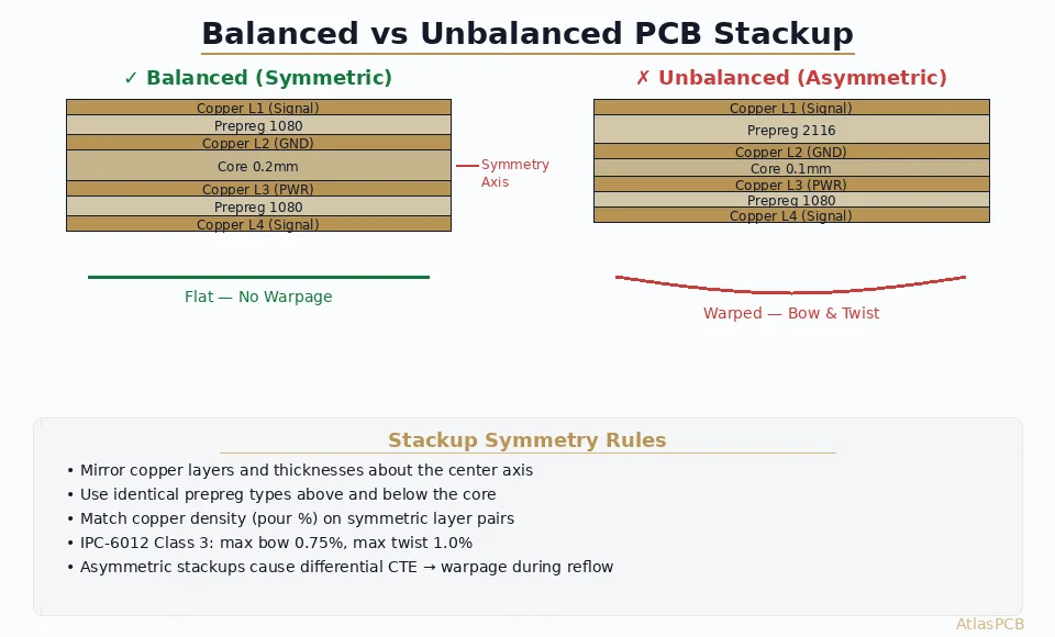
The fundamental principle of copper balancing relies on matching copper density between symmetric layer pairs across the board’s neutral axis (center). For an 8-layer PCB with layers L1 through L8:
- L1 must match L8 (outer pair)
- L2 must match L7 (first inner pair)
- L3 must match L6 (second inner pair)
- L4 must match L5 (core pair)
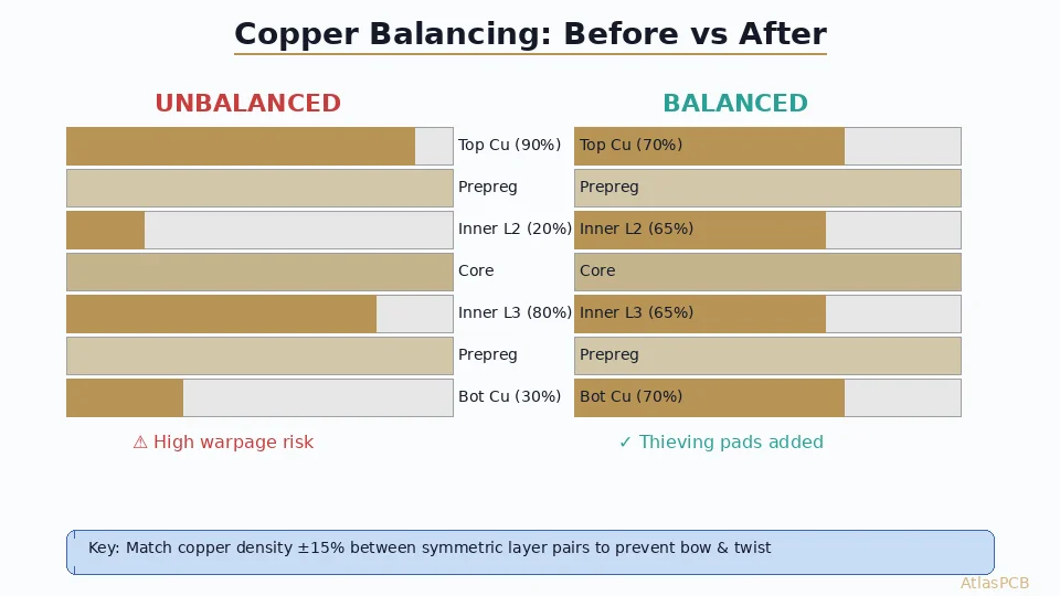
Each pair should have copper density within ±15% of each other. The “density” here refers to the percentage of a layer’s area covered by copper features (traces, pads, planes, pours, and thieving).
Measuring Copper Density
Most EDA tools provide built-in copper coverage analysis:
- Altium Designer: Reports → Board Information → Copper Area per Layer
- KiCad: Inspect → Board Statistics (per-layer fill percentage)
- Cadence Allegro: Route → Copper Analysis
- Siemens Xpedition: Manufacturing → Copper Balance Report
A typical multilayer board before optimization might show:
| Layer | Function | Coverage |
|---|---|---|
| L1 Top | Signal + Components | 35% |
| L2 | Ground Plane | 85% |
| L3 | Signal | 25% |
| L4 | Power Plane | 70% |
| L5 | Power Plane | 75% |
| L6 | Signal | 40% |
| L7 | Ground Plane | 88% |
| L8 Bot | Signal + Components | 45% |
The L3/L6 pair shows a 15% difference (acceptable) while L1/L8 shows a 10% difference (good). However, if L3 dropped to 15%, the asymmetry with L6 at 40% would create a 25% imbalance — well beyond the recommended threshold.
Copper Thieving Patterns and Design Rules
What Is Copper Thieving?
Copper thieving adds non-functional copper features to sparse layers to increase their copper density. These patterns serve no electrical purpose — they simply equalize the copper distribution to prevent mechanical deformation.
Common Thieving Pattern Types
1. Dot Array (Preferred for Signal Layers)
- Round pads 0.5-0.75 mm diameter
- Grid spacing: 1.0-1.27 mm (40-50 mil)
- Achieves approximately 15-25% additional coverage
- Minimal impact on signal coupling
2. Cross-Hatch Pattern
- Lines 0.2-0.3 mm wide at 45° angles
- Grid pitch: 1.0-2.0 mm
- Coverage: 30-50% depending on line width and pitch
- Commonly used on internal ground/power planes
3. Solid Fill (Ground Pour)
- Maximum coverage in non-signal areas
- Connected to ground net for EMC benefit
- Most effective for balancing but requires clearance management
- Best for reference plane layers
4. Snowflake Pattern
- Star-shaped features for uniform stress distribution
- Used in some advanced fabricators for thin substrates
- Less common but excellent thermal stress distribution
Design Rules for Thieving Placement
| Parameter | Recommendation |
|---|---|
| Minimum clearance to signals | 0.5 mm (20 mil) |
| Minimum clearance to pads | 0.25 mm (10 mil) |
| Distance from board edge | 0.5 mm minimum |
| Thieving in BGA field | Not recommended within via field |
| Connection to net | Ground (preferred) or floating |
| Clearance to controlled impedance traces | 3× trace width minimum |
Practical Implementation: CAD Workflow
Step 1: Analyze Current Copper Distribution
Before adding thieving, export copper coverage data for each layer. Most fabricators provide this analysis as part of DFM review, but designers should perform it pre-submission.
Step 2: Identify Critical Pairs
Calculate the density difference for each symmetric pair. Flag any pair with >15% difference for correction.
Step 3: Select Appropriate Pattern
- Signal layers (sparse): Dot array or floating copper islands
- Plane layers (already dense): Usually no thieving needed
- Mixed layers: Ground pour in open areas with dot array near signal routes
Step 4: Apply Thieving with Clearance Rules
In most EDA tools, this is accomplished through copper fill rules:
- Define a “thieving” net class with enlarged clearances
- Apply dot pattern or hatch in a special rule area
- Verify no DRC violations after thieving application
Step 5: Re-analyze and Iterate
After applying thieving, re-check copper density. Target each pair within ±10% for best results. Some iteration may be needed for boards with highly asymmetric signal routing.
Need Help with Copper Balancing for Your Multilayer PCB?
AtlasPCB provides free DFM copper balance analysis with every order. Our engineers optimize thieving placement for minimum warpage.
Get a Free DFM Review →IPC Standards for Bow and Twist
IPC-6012 Requirements
The IPC-6012 qualification standard defines maximum bow and twist limits:
- Class 2 (Standard): ≤1.5% of board diagonal for non-SMT, ≤0.75% for SMT
- Class 3 (High Reliability): ≤0.75% of board diagonal for all assemblies
- Class 3/A (Space/Military): ≤0.5% in some specifications
For a 200 mm × 150 mm board (diagonal = 250 mm):
- 0.75% limit = 1.875 mm maximum warpage
- 0.5% limit = 1.25 mm maximum warpage
IPC-2221 Design Guidance
IPC-2221B Section 10.4 recommends:
- Symmetric copper distribution about the board centerline
- Minimum 40% copper coverage on any layer in a multilayer construction
- Copper features on unused layer areas to balance the stackup
IPC-TM-650 Test Method 2.4.22
This test method defines how to measure bow and twist using a flat reference surface and height gauge. Fabricators perform this measurement on a statistical sample from each production lot.
Advanced Considerations
Thin Board Challenges (< 0.8 mm)
Thin PCBs used in mobile devices and wearables are extremely susceptible to warpage because the reduced board stiffness cannot resist thermomechanical stress. For boards under 0.8 mm total thickness:
- Tighten the balance tolerance to ±8%
- Use solid fills rather than dot patterns (more uniform stress)
- Consider asymmetric stackups with deliberate pre-cambering
- Specify low-CTE prepregs (Megtron 6, IS680)
High Layer Count Boards (16+ Layers)
With more layers, each pair contributes less individual stress, but cumulative effects can still cause issues. For 16+ layer boards:
- Focus on outer 4 layer pairs (highest stress contribution)
- Inner pairs can tolerate up to ±20% difference
- Core pairs (center) have minimal influence on surface warpage
- Copper balance is especially critical for signal layer pairs adjacent to the outer layers
Panel-Level Balancing
Some fabricators perform panel-level copper balancing, adding thieving in the panel frame and between individual board images. This is particularly important for:
- Boards with very low copper density on one side
- Long narrow boards prone to bow along the length
- Panels with mixed board designs (different copper per design)
Relationship to Other DFM Factors
Copper balancing works alongside several other DFM considerations:
- Stackup symmetry: Material type and thickness symmetry complements copper balancing
- Warpage control: Pre-baking, press cycle optimization, and material selection
- PCB bow and twist measurement: Quantifying results of balancing efforts
- Multilayer stackup design: Overall design framework that includes copper balance as one factor
Copper Balancing Checklist for Designers
Before submitting your design to fabrication, verify:
- ✅ Copper density analyzed for all layers
- ✅ Symmetric pairs within ±15% (±10% for thin boards)
- ✅ Thieving patterns applied with proper clearances
- ✅ No thieving within BGA via fields
- ✅ Controlled impedance traces have 3× clearance to thieving
- ✅ Thieving connected to ground or confirmed floating
- ✅ Final DRC clean after thieving application
- ✅ Fab notes specify “maintain copper thieving as designed”
Conclusion
Copper balancing is one of the most cost-effective DFM practices available — it costs nothing in additional fabrication steps while dramatically reducing yield loss from warpage. By maintaining symmetric copper distribution within ±15% between layer pairs and applying appropriate thieving patterns in sparse areas, designers prevent the thermomechanical stress that causes bow and twist during lamination and reflow.
For complex multilayer boards where copper balance proves difficult through thieving alone, consider discussing stackup modifications or alternative materials with your fabricator early in the design process.
Ready to optimize your multilayer PCB for minimal warpage? AtlasPCB’s engineering team includes copper balance analysis in every DFM review. Upload your Gerber files and receive a detailed copper distribution report within 24 hours. Get started with a quote →
About AtlasPCB — We specialize in complex PCB manufacturing for HDI, RF, and high-reliability applications. Explore our multilayer PCB fabrication up to 30 layers, free engineering DFM review, or get an full PCB manufacturing capabilities . Every order includes free engineering review. Get your quote.
Reviewed by AtlasPCB Engineering Team — IPC-certified manufacturing specialists with 15+ years of production experience in HDI, RF, and high-reliability PCB fabrication. Content based on factory floor data and real customer design reviews.
- copper balancing
- copper thieving
- PCB warpage
- multilayer PCB
- DFM
- IPC-2221
- bow and twist
- PCB manufacturing
- lamination