· AtlasPCB Engineering · Engineering · 7 min read
Quilter AI Proves Autonomous PCB Layout Works: Project Speedrun Delivers a Working Single-Board Computer
How Quilter.ai's Project Speedrun validated AI-powered PCB layout by autonomously placing and routing a complete NXP i.MX 8M Mini SBC with LPDDR4 — demonstrating production-ready AI layout for real hardware.

The Skeptic’s Challenge — Answered
The AI-powered PCB layout space has faced persistent skepticism from experienced hardware engineers. The criticism is legitimate: most demonstrations have involved simple evaluation boards or reference designs specifically chosen to highlight AI tool capabilities. The two recurring challenges from working layout designers are:
- “AI can’t handle real-world board complexity” — Demonstrations use curated, simple designs
- “Show me working hardware, not pretty pictures” — Marketing renders don’t prove electrical functionality
Quilter.ai decided to address both challenges simultaneously with Project Speedrun: a complete, working single-board computer designed entirely by their autonomous layout engine, fabricated, assembled, and validated by booting into a Linux desktop.
This isn’t a hypothetical demonstration. EE Journal’s Max Maxfield confirmed in his May 2026 column that the Quilter-designed board “boots, runs a browser, and behaves exactly as a single-board computer should.” The PCB design community can independently verify the results because the NXP i.MX 8M Mini reference design documentation is publicly available for comparison.
Why a Single-Board Computer?
Choosing the Right Validation Target
The Quilter team made deliberate choices about their validation target:
Why an SBC:
- Widely understood design class — engineers can immediately assess layout quality
- Inherently challenging from a layout perspective (processor, memory, multiple I/O standards)
- Easy to verify functionality (does it boot? does it run Linux?)
- Comparable to commercially available products (Raspberry Pi-class complexity)
Why NXP i.MX 8M Mini:
- Mature processor ecosystem with known-good schematics
- LPDDR4 memory interface — one of the most demanding routing challenges
- Multiple I/O standards (USB, Ethernet, MIPI, I2C, SPI, UART)
- Publicly available documentation for independent verification
What they deliberately avoided:
- Inventing a new product (would introduce software/driver development distractions)
- Using a trivially simple design (wouldn’t address skeptics’ concerns)
- Selecting a design that plays to AI strengths while hiding weaknesses
The LPDDR4 Challenge
Anyone who has manually routed DDR memory interfaces understands why this is significant. LPDDR4 routing requires:
- Length matching: Data, address, and clock signals must be matched to within tight tolerances (typically ±5-10 mils within a byte lane)
- Impedance control: 40Ω single-ended, 80Ω differential impedance targets with ±10% tolerance
- Reference plane continuity: Return current paths must be maintained across all layer transitions
- Spacing rules: Strict crosstalk isolation between byte lanes and between command/data groups
- Via constraints: Controlled via transitions with proper anti-pad sizing and stitching
- Stackup optimization: Layer assignment directly affects routing feasibility and signal integrity
Traditionally, DDR routing is where junior layout designers struggle and where senior designers earn their premium rates. Successfully automating this demonstrates genuine engineering understanding in the AI system — not just simple maze-routing capability.
How Quilter’s Approach Works
Philosophy: Augment, Don’t Replace
Quilter takes a fundamentally different approach from AI companies trying to automate the entire design process (“give me a prompt and I’ll generate complete hardware”). Their position:
- Humans architect the system: Engineers choose components, design the schematic, define the architecture
- Humans define constraints: Impedance requirements, spacing rules, keep-out zones, mechanical boundaries
- AI handles physical implementation: Component placement, routing, layer assignment, via optimization
This division of labor makes sense because:
- Architecture decisions require market knowledge, component ecosystem expertise, and system-level thinking that current AI cannot reliably provide
- Physical implementation (placement + routing) is primarily an optimization problem — well-suited to AI
- Engineers maintain full control over the design intent while eliminating their most time-consuming task
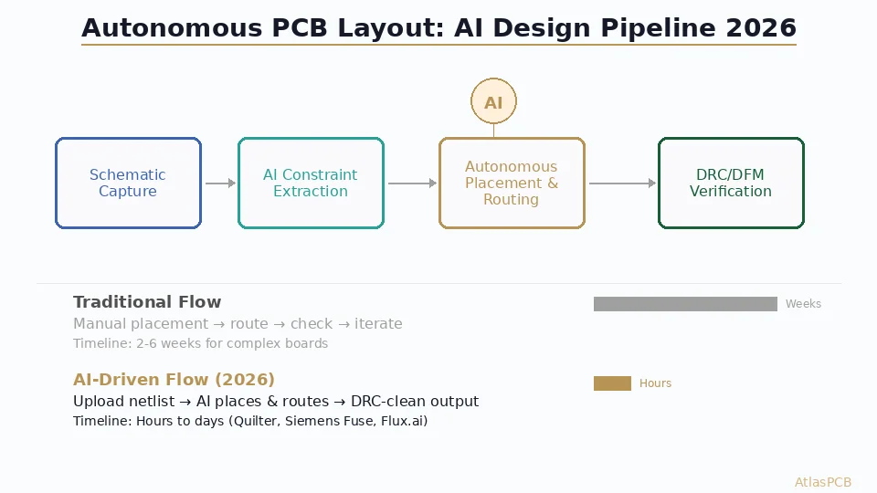
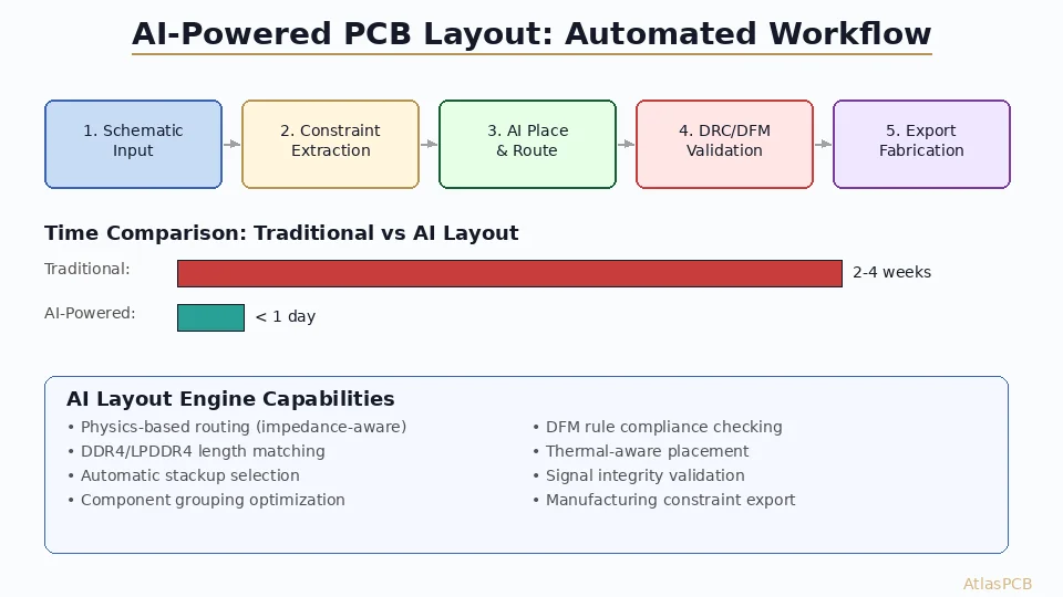
The AI Layout Process
Step 1: Design Import Upload the schematic and constraint set. Quilter’s “circuit comprehension” engine parses the design to understand:
- Net classes and their signal integrity requirements
- Component groupings and placement preferences
- Mechanical constraints (board outline, keep-outs, mounting holes)
- Electrical rules (clearances, impedance targets, length matching groups)
Step 2: Constraint Interpretation Rather than requiring manual constraint definition for every net (as traditional EDA tools do), Quilter infers constraints from the circuit topology:
- Identifies DDR interfaces and auto-applies length matching
- Recognizes power delivery networks and plans appropriate copper weight
- Detects high-speed differential pairs and assigns impedance targets
- Groups related components for placement optimization
Step 3: Autonomous Layout The AI performs placement and routing simultaneously (not sequentially as human designers typically work):
- Component placement optimized for routability, thermal performance, and mechanical constraints
- Multi-layer routing with automatic layer assignment based on signal characteristics
- Stackup selection based on impedance requirements and manufacturing feasibility
- Iterative refinement to meet all constraints simultaneously
Step 4: DRC/DFM Validation The complete layout is verified against:
- Design Rule Check (DRC) — spacing, width, annular ring compliance
- Electrical Rule Check (ERC) — net connectivity, antenna violations
- DFM analysis — manufacturer-specific capability limits
- Signal integrity — impedance, length matching, crosstalk verification
AI-Designed Boards Still Need Expert Fabrication
Whether your layout is manual or AI-generated, AtlasPCB delivers precision manufacturing with engineering review on every order.
Upload Your Design →Industry Implications
Time-to-Market Compression
The traditional PCB design timeline for a board of Speedrun’s complexity:
- Schematic capture: 1-2 weeks
- Layout (placement + routing): 2-4 weeks ← AI automates this
- Design review and iteration: 1 week
- Fabrication: 1-3 weeks
- Assembly and test: 1-2 weeks
Automating the layout phase compresses the total development cycle by 2-4 weeks — representing a 25-40% reduction in time-to-prototype. For companies iterating on hardware designs, this means additional prototype cycles within the same schedule.
Workforce Impact
Rather than eliminating PCB designers, AI layout tools shift their role:
- From: Spending 80% of time on mechanical routing tasks
- To: Spending 80% of time on architecture, constraint definition, review, and optimization
This is analogous to how CAD tools didn’t eliminate draftsmen — they transformed drafting roles into design engineering roles. The value moves upstream from implementation to intent.
Fabrication Requirements Don’t Change
An important point for PCB manufacturers: AI-designed boards use the same materials, processes, and standards as manually-designed boards. The fabrication challenge doesn’t change based on whether a human or AI performed the layout. Manufacturing capabilities — trace/space minimums, drill sizes, layer counts, materials — remain the determining factors in whether a design can be built.
What may change:
- AI tools may produce more routing-optimal designs (shorter trace lengths, more efficient layer utilization)
- AI may better utilize manufacturing capabilities (using tighter tolerances where available, relaxing where not critical)
- Designs may be DFM-compliant from the start rather than requiring iterative DFM review
The Broader EDA AI Landscape
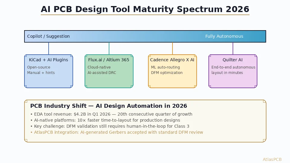
Quilter isn’t alone. The AI-powered PCB design space now includes:
- Quilter: Autonomous placement and routing (the most production-proven for layout)
- Flux.ai: Cloud-native design with AI assistance across the workflow
- Cadence Allegro AI: Machine learning for route optimization within their traditional platform
- Siemens Xpedition: AI-powered front-end design entry and manufacturing connection
- Altium 365: Cloud collaboration with emerging AI features
The EDA industry is converging on AI as a fundamental tool — not a novelty feature. PCB East 2026 attendance was up 48% year-over-year, with AI infrastructure driving much of the interest.
What This Means for Hardware Engineers
Short-Term (2026-2027)
- AI layout tools are ready for production use on moderately complex designs (4-8 layers, single processor, standard interfaces)
- DDR4/5 routing capability is validated but may need human review for cutting-edge designs (HBM interposers, 28G SerDes)
- Adoption will accelerate among hardware startups where layout engineer availability is limited and time-to-market is critical
Medium-Term (2027-2029)
- AI tools will handle 90%+ of standard PCB layouts without human intervention
- Human experts will focus on extreme designs: 30+ layers, RF/microwave, flex-rigid, exotic materials
- Design iteration cycles will compress from weeks to hours for standard complexity boards
- “AI-designed” will become as unremarkable as “CAD-designed” — just how things are done
Long-Term (2030+)
- Full system-level optimization: AI considers manufacturing constraints, supply chain availability, and cost simultaneously during design
- Real-time DFM feedback from specific factories: AI designs directly for the intended manufacturer’s exact capabilities
- Generative design exploration: “Design 10 board variants optimized for different cost/performance trade-offs” becomes possible
Further Reading
- AI-Powered DFM Checking for PCB Design
- Signal Integrity PCB Design Guide
- HDI PCB Design Guide
- PCB Via Transitions and Return Current Paths
Whether your board was designed by a human expert or an AI engine, AtlasPCB manufactures with the same precision engineering review. Get a quote for your next project.
About AtlasPCB — We specialize in complex PCB manufacturing for HDI, RF, and high-reliability applications. Explore our full PCB manufacturing capabilities, or get an instant online quote . Every order includes free engineering review. Get your quote.
Reviewed by AtlasPCB Engineering Team — IPC-certified manufacturing specialists with 15+ years of production experience in HDI, RF, and high-reliability PCB fabrication. Content based on factory floor data and real customer design reviews.
- AI PCB design
- autonomous layout
- Quilter AI
- PCB automation
- EDA tools
- machine learning routing
- DDR4 layout
- PCB design productivity