· AtlasPCB Engineering · Engineering · 9 min read
PCB Via Transitions and Return Current Paths: A Signal Integrity Design Guide
Master via transitions in multi-layer PCBs by understanding return current behavior, reference plane changes, and stitching via placement to minimize EMI and preserve signal quality.

Understanding Via Transitions in High-Speed PCB Design
Every multi-layer PCB design involves routing signals between layers. Whether you’re escaping a BGA pad field, transitioning from a microstrip to a stripline, or connecting components on opposite sides of the board, vias are the vertical interconnects that make it possible. But every via transition introduces a fundamental challenge that many designers overlook: what happens to the return current when the signal changes layers?
At PCB East 2026, Rick Hartley — one of the industry’s foremost signal integrity educators — reinforced this principle across multiple sessions: “The return current doesn’t care about your stackup intentions. It follows physics. If you don’t provide a path, it will find one — and that path will radiate.” This concept, simple in theory but complex in practice, forms the foundation of EMI-compliant high-speed PCB design.
The challenge becomes critical as data rates increase. At 1 Gbps, a return current path disruption might cause minor ringing. At 28 Gbps (PAM4 signaling common in AI/HPC applications), the same disruption causes bit errors, timing violations, and compliance failures. Understanding and managing return current behavior at via transitions is no longer optional — it’s a requirement for any design operating above 1 GHz.
The Physics of Return Current at Layer Transitions
How Return Current Actually Flows
Contrary to common misconception, return current does not simply flow back through the nearest ground pin. At high frequencies, return current follows the path of least impedance — which is the path directly beneath (or above) the signal trace on the nearest reference plane. This creates the smallest possible loop area, minimizing inductance and therefore impedance.
For a microstrip trace on Layer 1 referenced to a ground plane on Layer 2, the return current flows on the Layer 2 ground plane surface directly beneath the trace. The current density distribution follows a well-defined pattern — approximately 95% of the return current flows within ±3× the trace-to-plane distance on either side of the trace.
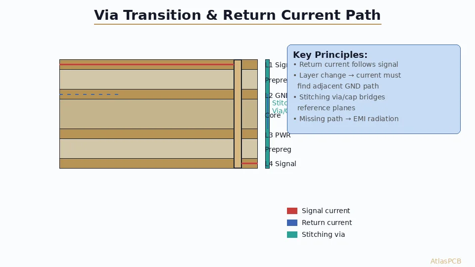
What Happens at a Via Transition
When a signal via carries the signal from Layer 1 (referenced to L2 GND) to Layer 4 (referenced to L3 PWR), two things must happen:
- The signal current flows through the via barrel from L1 to L4
- The return current must transition from the L2 GND plane to the L3 PWR plane
If L2 GND and L3 PWR are not connected near the via, the return current must travel laterally across the plane to find a connection point. This dramatically increases the current loop area — and loop area directly correlates with radiated emissions (EMI) and susceptibility to external noise.
The relationship is quantifiable. The inductance of a current loop is proportional to the enclosed area:
L ≈ μ₀ × Area / length
Doubling the loop area approximately doubles the inductance, which increases the impedance discontinuity and the radiated field strength.
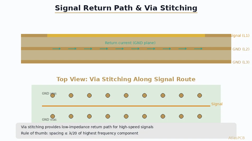
The Three Reference Plane Scenarios
Scenario 1: Same reference plane (ideal) Signal transitions from L1 stripline (ref L2 GND) to L3 stripline (ref L2 GND). The return current stays on the same plane — no transition needed. This is the lowest-risk via transition.
Scenario 2: GND-to-GND transition Signal moves between layers referencing different ground planes (e.g., L2 GND to L5 GND). A stitching via connecting the two ground planes provides a direct return path. This is the second-best scenario.
Scenario 3: GND-to-power transition (highest risk) Signal moves from a GND-referenced layer to a power-referenced layer. The planes are DC-isolated by design. A decoupling capacitor must bridge the return current between planes.
Stitching Via Design Guidelines
Placement Rules
The effectiveness of a stitching via depends primarily on its proximity to the signal via. Industry best practices, reinforced by electromagnetic simulation and validated at conferences like PCB East 2026, establish these guidelines:
| Signal Frequency | Maximum Distance | Recommended Distance |
|---|---|---|
| < 1 GHz | 200 mils (5 mm) | 100 mils (2.5 mm) |
| 1–5 GHz | 100 mils (2.5 mm) | 50 mils (1.27 mm) |
| 5–15 GHz | 50 mils (1.27 mm) | 20 mils (0.5 mm) |
| > 15 GHz | 20 mils (0.5 mm) | Adjacent (via-in-pad) |
Via Configuration Strategies
Single stitching via: Minimum approach. Place one ground via within the specified distance of the signal via. Provides a single return current path.
Paired stitching vias: Place two ground vias on either side of the signal via. Reduces inductance by providing parallel return paths. Preferred for signals > 5 GHz.
Via fence: For differential pairs or critical single-ended signals > 10 GHz, surround the signal via(s) with a ring of ground vias. This provides a coaxial-like transition structure with controlled impedance through the via region.
Decoupling Capacitor Selection for Power-Ground Bridging
When the signal transitions between a ground-referenced layer and a power-referenced layer, a stitching via alone won’t work (you can’t short VCC to GND). Instead, use a decoupling capacitor:
- Capacitor value: 100 nF for frequencies below 500 MHz; 10 nF for 500 MHz–2 GHz; 1 nF or lower for above 2 GHz
- Package size: 0201 or 01005 preferred (lowest parasitic inductance)
- Placement: Capacitor pads should be within 50 mils of the signal via, with short, wide traces to the planes
- Via connection: Use two vias per pad (one to each plane) for lowest inductance
The self-resonant frequency (SRF) of the capacitor must exceed the signal’s fundamental frequency. Above the SRF, the capacitor becomes inductive and ceases to provide a low-impedance path.
Need Expert Signal Integrity Review?
AtlasPCB provides DFM analysis including return current path verification for high-speed designs up to 28 Gbps.
Get Engineering Review →Modeling Via Transition Impedance
Via Stub Effects
Beyond return current path concerns, via stubs create resonant structures that cause signal degradation at specific frequencies. A via stub is the unused portion of a through-hole via extending beyond the target signal layer.
The resonant frequency of a stub is:
f_res = c / (4 × stub_length × √εr)
For a typical 62-mil (1.57 mm) total board thickness with a signal on Layer 2 and a stub extending to Layer 8, the stub length is approximately 1.2 mm. With FR-4 (εr ≈ 4.2), the first resonance occurs around:
f_res = 3×10⁸ / (4 × 0.0012 × √4.2) ≈ 30.5 GHz
For designs operating at 25–28 Gbps (PAM4), harmonics of the signal can excite this resonance. Solutions include:
- Back-drilling: Mechanically removing the stub after fabrication (standard for ≥ 10 Gbps designs)
- Blind/buried vias: Use HDI construction to eliminate stubs entirely
- Via-in-pad: Laser-drilled microvias connecting only adjacent layers
Impedance Through the Via Barrel
The characteristic impedance of the via barrel is typically 30–50 Ω for a standard through-hole via with surrounding ground vias, compared to the 50 Ω or 100 Ω (differential) trace impedance. This mismatch creates reflections.
Strategies to control via impedance:
- Adjust antipad diameter: Larger antipad = higher impedance. Typical range: 20–50 mils diameter
- Use ground via cage: Surrounding ground vias create a coaxial structure with more controlled impedance
- Optimize pad size: Minimize signal via pad on non-functional layers (teardrops only on signal layers)
Practical Design Workflow
Step 1: Identify Critical Signal Transitions
Before routing, identify all signals that will require layer changes:
- DDR4/5 address, data, clock, and strobe signals
- SerDes lanes (PCIe, USB, Ethernet)
- Clock distribution networks
- Any single-ended signal > 500 MHz or differential pair > 1 Gbps
Step 2: Plan Reference Plane Assignments
Map which layers reference which planes. The ideal stackup minimizes the number of GND-to-power transitions:
L1: Signal (ref L2 GND)
L2: GND
L3: Signal (ref L2 GND) ← Same reference, easy transition from L1
L4: PWR (VCC)
L5: Signal (ref L4 PWR) ← Power reference, needs cap if coming from L3
L6: GND
L7: Signal (ref L6 GND)
L8: Signal (ref L6 GND)
Step 3: Place Stitching Vias During Routing
Most modern EDA tools allow you to define rules that automatically flag signal vias lacking nearby stitching connections. Configure these rules early:
- Set proximity constraints based on signal speed class
- Define via types (stitching via drill size typically 8–10 mil for HDI)
- Enable DRC checking for return current path compliance
Step 4: Simulate and Verify
For critical nets (> 5 Gbps), perform 3D electromagnetic simulation of the via transition region:
- Extract S-parameters for the complete transition (trace → via → trace)
- Verify insertion loss (S21) meets link budget requirements
- Check return loss (S11) is below -15 dB at the fundamental frequency
- Confirm crosstalk between adjacent vias (S31) is within specification
Common Design Mistakes
Mistake 1: Split Reference Planes Under Signal Traces
Cutting a slot in a reference plane (for routing on an inner layer, for example) forces return current to detour around the slot. This is equivalent to a missing stitching via — but worse, because the detour affects the entire trace length crossing the split.
Solution: Never route signals across reference plane splits. If a split is unavoidable, route signals on a different layer or bridge the split with a stitching capacitor directly at the crossing point.
Mistake 2: Relying Only on Board-Edge Ground Vias
Some designers place ground vias only at the board perimeter, assuming the planes will distribute return current adequately. For signals > 100 MHz, this creates unacceptably large loop areas for any via transition located away from the edge.
Solution: Distribute stitching vias throughout the board, with higher density near signal via clusters (BGA breakout regions, connector areas).
Mistake 3: Ignoring Power Plane Return Current
When using a power plane as a reference, many designers forget that AC return current can flow on power planes. The plane functions identically to a ground plane at high frequencies — the DC voltage is irrelevant for AC signal return current.
Solution: Ensure adequate decoupling between power and ground planes (plane capacitance + discrete capacitors) so that return current can flow on whichever plane is the nearest reference.
Impact on EMI Compliance
Return current path management directly affects electromagnetic compatibility (EMC) test results. A single poorly managed via transition can cause a 10–20 dB increase in radiated emissions at the signal frequency.
For pre-compliance estimation, the electric field strength from a current loop at distance d is:
E ≈ 1.32 × 10⁻¹⁴ × (f² × A × I) / d
Where:
- f = frequency (Hz)
- A = loop area (m²)
- I = current amplitude (A)
- d = measurement distance (m)
This shows that radiated emissions increase with the square of frequency. A 5× increase in signal frequency (e.g., from 1 GHz to 5 GHz) results in 25× higher field strength — making return current path management exponentially more critical for modern high-speed designs.
Further Reading
- Via-in-Pad Plated Over (VIPPO) Design Guide
- RF Via Transitions for Microwave PCB Design
- Signal Integrity PCB Design Guide
- PCB Thermal Via Array Design
Need help with high-speed PCB stackup planning and via transition optimization? Contact our engineering team for a comprehensive design review.
About AtlasPCB — We specialize in complex PCB manufacturing for HDI, RF, and high-reliability applications. Explore our impedance-controlled PCB manufacturing . Every order includes free engineering review. Get your quote.
Reviewed by AtlasPCB Engineering Team — IPC-certified manufacturing specialists with 15+ years of production experience in HDI, RF, and high-reliability PCB fabrication. Content based on factory floor data and real customer design reviews.
- signal integrity
- via transition
- return current
- PCB design
- EMI
- stitching via
- reference plane
- ground plane