· AtlasPCB Engineering · Engineering · 9 min read
LLM-Assisted PCB Design Review: How AI Copilots Are Reducing Respins in 2026
Practical assessment of AI/LLM-powered design review tools for PCB engineers — what works today, what does not, and how to integrate AI copilots into your DFM workflow without over-trusting automation.
The Current State: What AI Actually Does in PCB Review
The PCB industry has moved beyond the hype phase for AI-assisted design tools. In 2026, the practical reality is that AI copilots handle the tedious, repetitive portion of design review — geometric rule checking at scale — while human engineers focus on the judgment-intensive 20% that machines still get wrong. This division of labor is not a compromise; it is genuinely optimal for both speed and quality.
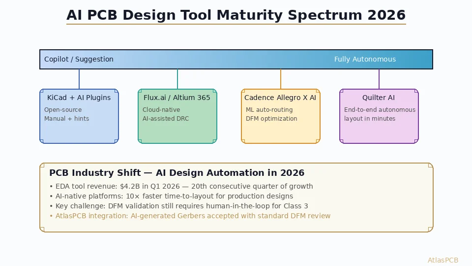
The tools that work today fall into two categories. First, enhanced DRC engines that use trained neural networks to identify violations beyond what traditional rule decks catch: acid traps that pass minimum clearance but will trap etchant, copper slivers that pass DRC but will delaminate in thermal cycling, and solder mask openings that technically meet spec but create inspection escapes on AOI lines. Second, generative recommendation engines that suggest routing alternatives, via fanout patterns, and decoupling placement based on millions of previously manufactured boards.
What none of these tools do — and this is critical for engineers evaluating them — is understand your design intent. An AI can tell you that your differential pair spacing violates a rule. It cannot tell you whether your power delivery network provides adequate decoupling for a 100A transient at the point of load. That distinction determines how you integrate AI into your workflow: as a first-pass filter that catches the obvious 80%, not as a replacement for engineering expertise.
ENGINEERING-DRIVEN DFM
AI-Enhanced DFM Review on Every Order
Our engineering team combines automated checking with hands-on review — catching what AI alone misses.
Submit Design for Review ›Where AI Copilots Excel: The 85% Automation Zone
The categories of design violations that AI handles better than humans are precisely those that involve checking thousands of instances against defined criteria. A human reviewer’s attention fades after checking the 200th via clearance. A machine checks all 8,000 vias with equal rigor in under 10 seconds.
Geometric DRC at scale. Modern AI-driven DRC engines process a 16-layer, 10,000-net design in under 60 seconds — a task that would take a manual reviewer 6-8 hours to complete with equivalent thoroughness. More importantly, they catch edge cases that traditional rule decks miss. A standard DRC checks minimum annular ring. An AI-trained DRC additionally flags annular rings that are technically compliant but adjacent to a high-current trace where thermal expansion will stress the via barrel during reflow — a reliability failure mode that only becomes apparent in production.
Pattern recognition from manufacturing data. The most powerful AI DFM tools train on actual manufacturing defect databases. When your design contains a pad geometry that has historically generated 3x the average solder void rate, the AI flags it — not because it violates a rule, but because empirical production data shows it correlates with assembly defects. This is something no static rule deck can capture because it requires learning from real-world manufacturing outcomes.
Design-for-test violations. AI can instantly verify that every net is accessible for testing (either through a test pad or via ICT-accessible via), that component orientations are consistent (reducing placement error), and that BGA pad sizes match recommended land patterns from component datasheets. These checks are tedious for humans but trivial for pattern-matching algorithms.
In our fabrication facility, we deployed AI-assisted Gerber review on incoming orders in Q1 2026. The system catches an average of 12 additional issues per design that our previous rule-based checking missed — mostly copper slivers under 2 mil, non-functional pads that would interfere with wave solder, and solder mask registration risks on fine-pitch QFN packages. These catches save our customers roughly $2,000-5,000 per avoided respin.
Where AI Still Fails: The Critical 15% Requiring Human Judgment
The failure modes of AI design review cluster around decisions that require understanding the design’s purpose, operating environment, and physics that extend beyond geometry.
Signal integrity and coupling assessment. An AI can check that your differential pair spacing is 5 mil (meeting the rule). It cannot determine whether the aggressor trace running parallel for 3 inches on the adjacent layer will create unacceptable far-end crosstalk at 16 Gbps. That calculation requires understanding the entire signal path — driver impedance, receiver sensitivity, frequency content, and return path continuity. Tools like HyperLynx and Ansys SIwave still require human setup and interpretation for meaningful SI analysis.
Thermal management adequacy. AI cannot assess whether your thermal via array under a 5W power IC will maintain junction temperature below 85C in a sealed enclosure with no airflow. That determination requires thermal simulation (ICEPAK, FloTHERM) with boundary conditions that only the system engineer knows. The AI might flag that you have “fewer thermal vias than typical” — but “typical” might be completely wrong for your specific thermal budget.
Manufacturability at your specific fabricator. Every PCB factory has unique capabilities and limitations that go beyond published specs. Our minimum trace width is 3 mil, but achieving 3 mil reliably on inner layers of a 24-layer board requires specific process controls that differ from 3 mil on a 4-layer board. A general-purpose AI DFM tool treats all 3-mil traces equally. An experienced process engineer at a specific fabricator knows which designs need additional attention.
Design intent violations. The most insidious errors are designs that pass all geometric rules but violate their own intent. A ground plane with a slot cut by a routing channel creates a return path discontinuity that causes EMI — but the AI sees a copper pour that meets minimum width requirements and passes it. Only a human reviewing the design holistically catches that the slot breaks a critical return path.
BEYOND AUTOMATED CHECKS
Human Engineering Review for Complex Designs
HDI, RF, and high-speed designs need experienced eyes — not just rule checking. Our team reviews for signal integrity and manufacturability.
Practical Integration: A Workflow That Works
Based on what we observe from customers who have successfully integrated AI into their design flow, here is the workflow that delivers the best results:
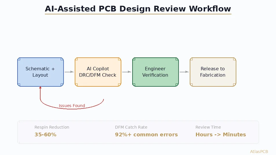
Phase 1: Continuous AI checking during layout (real-time). Run the AI DRC engine incrementally as you route. This catches violations immediately — before they propagate through the design. Modern EDA integrations (Siemens Xpedition AI Advisor, Cadence iDFM) can check placement and routing decisions against manufacturing rules in real-time, with sub-second feedback as you draw traces.
Phase 2: Full AI audit at design freeze (30-60 minutes). Once routing is complete, run the comprehensive AI DFM suite that checks everything: all layers simultaneously, inter-layer interactions, stackup consistency, manufacturing panel constraints, and assembly requirements. This catches the issues that incremental checking misses — particularly multi-layer interactions like via-to-buried-via clearances and power plane split proximity to signal transitions.
Phase 3: Human engineering review (2-4 hours for complex boards). An experienced engineer reviews the AI findings, dismisses false positives, and then conducts the context-dependent checks that AI cannot perform: SI/PI assessment, thermal review, EMC compliance check, and fabricator-specific manufacturability evaluation. This phase is shorter because the AI has already eliminated the geometric noise.
Phase 4: Fabricator DFM feedback (24-48 hours). Your chosen fabricator runs their own internal checks against their actual process capabilities. This is where factory-specific knowledge applies — press parameters, drilling accuracy at volume, and registration tolerances on their specific equipment. Smart fabricators now combine AI screening with experienced process engineering review.
The cumulative effect: designs that previously required 2-3 spins to reach production maturity now achieve it in 1-2 spins. At $3,000-15,000 per spin (NRE, prototyping, testing, and engineering time), even a single avoided respin justifies the annual cost of AI design tools many times over.
The ROI Calculation: Is AI Design Review Worth the Investment?
For engineering teams evaluating whether to adopt AI-assisted DFM tools, the math is straightforward. The typical hardware startup spends $5,000-15,000 per board revision when you account for prototype fabrication, assembly, engineering time for debugging, and schedule impact. Industry data from 2025-2026 shows that first-spin success rates for complex boards (8+ layers, fine-pitch BGA, controlled impedance) sit around 40-60% without AI assistance and 70-85% with it.
If your team releases 4 new designs per year, improving first-spin success from 50% to 80% eliminates 1.2 respins per year on average. At $8,000 per respin, that is $9,600 in direct savings — far exceeding the $2,000-5,000 annual cost of AI DFM tools. The schedule benefit compounds this further: each avoided respin saves 3-6 weeks of calendar time, which translates to faster time-to-market and earlier revenue recognition.
For companies using external fabrication services like ours, the AI review integrated into the fabricator’s front-end engineering process comes at no additional cost — it simply reduces the back-and-forth query cycle and gets your boards into production faster. Our internal AI screening catches an average of 4.3 actionable issues per new design that would otherwise become engineering queries, saving 2-3 days of communication overhead per order.
ATLASPCB
Reduce Your Respin Risk — Submit Your Design
AI-enhanced screening plus experienced process engineers. We catch issues before they become expensive problems.
Upload Gerber and Get Quote ›Reviewed by AtlasPCB Engineering Team — 15+ years in advanced PCB fabrication for RF, HDI, and rigid-flex applications.
Related Reading:
About AtlasPCB — We specialize in complex PCB manufacturing for HDI, RF, and high-reliability applications. Explore our free engineering DFM review . Every order includes free engineering review. Get your quote.
Reviewed by AtlasPCB Engineering Team — IPC-certified manufacturing specialists with 15+ years of production experience in HDI, RF, and high-reliability PCB fabrication. Content based on factory floor data and real customer design reviews.
- ai-pcb-design
- dfm
- eda-tools
- design-review