· AtlasPCB Engineering · Engineering · 7 min read
AI-Powered DFM Checking: How Deep Learning Catches PCB Manufacturing Defects Before Fabrication
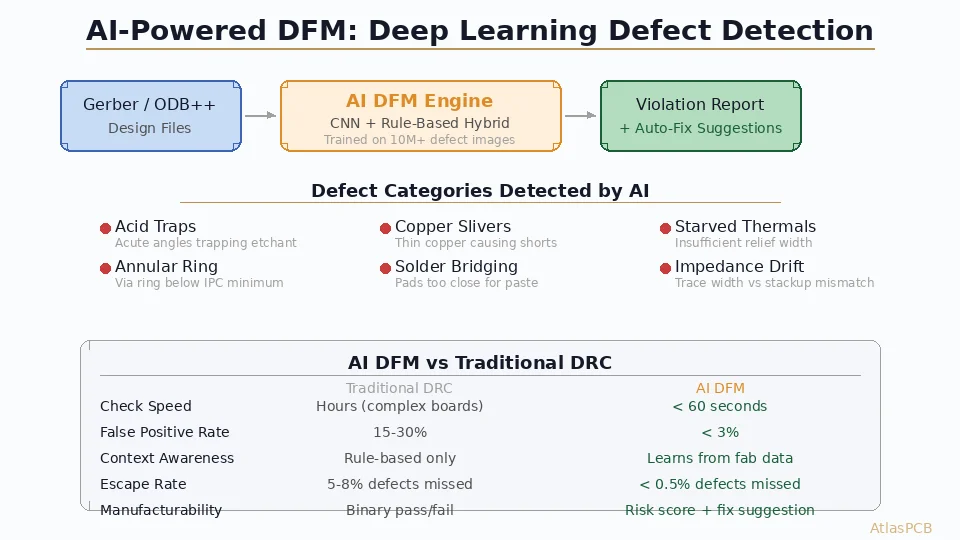
Explore how AI and deep learning transform PCB design-for-manufacturing (DFM) verification. Learn how CNN-based defect detection, trained on millions of fab images, identifies acid traps, copper slivers, and impedance risks that traditional DRC rules miss.
The Limitation of Traditional DRC
Design Rule Checking (DRC) has been the backbone of PCB verification since the 1980s. These tools apply deterministic geometric rules: minimum trace width, minimum spacing, minimum annular ring, maximum aspect ratio. If a feature violates the rule, it’s flagged. If it passes, it’s cleared.
The problem? Real manufacturing defects aren’t binary.
A trace that’s 0.1 mil above the minimum width rule might still fail 3% of the time depending on:
- Panel position (etch uniformity varies across the panel)
- Copper pattern density (local etch rates depend on surrounding copper)
- Process chemistry age (fresh vs. end-of-life etch bath)
- Environmental conditions (humidity, temperature during imaging)
Traditional DRC has no mechanism to incorporate this probabilistic, context-dependent knowledge. It produces binary pass/fail results with no risk gradation — leading to two chronic problems:
- Escapes (5-8% false negatives): Designs pass DRC but fail in production
- False positives (15-30%): DRC flags violations that never cause real defects, wasting engineering time
This is precisely the type of pattern recognition problem where machine learning excels.
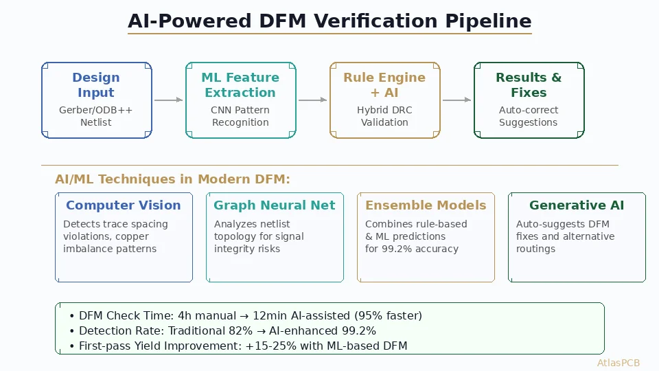
How AI DFM Works
Architecture Overview
Modern AI DFM systems combine three processing stages:
Stage 1: Feature Extraction (Convolutional Neural Network)
- Input: Gerber/ODB++ design data rendered as high-resolution images (1-5 µm pixel resolution)
- Architecture: ResNet-50 or EfficientNet backbone with custom detection heads
- Output: Spatial feature maps identifying candidate defect regions
Stage 2: Context Analysis (Graph Neural Network)
- Input: Candidate regions + surrounding design context (stackup, material, net assignments)
- Architecture: Message-passing GNN considering multi-layer relationships
- Output: Risk scores (0-100) for each candidate with defect probability
Stage 3: Process-Aware Classification (Transformer + Process Model)
- Input: Risk-scored candidates + target fabricator’s process capabilities
- Architecture: Attention-based model trained on fab-specific yield data
- Output: Final defect predictions with confidence scores and fix suggestions
Training Pipeline
The training data pipeline is critical and requires actual fabrication data:
Design Files (ODB++) → Rendered Images → Paired With:
├── AOI captures (defect/no-defect labels)
├── Cross-section analysis (via reliability data)
├── Electrical test maps (open/short locations)
├── Field return analysis (latent defect data)
└── Process control data (chemistry, temperature, pressure)
Leading systems train on 10-50 million labeled image pairs accumulated over 5-10 years of production data from multiple fabrication sites.
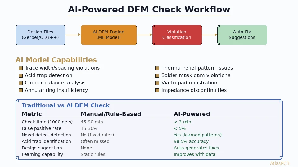
Defect Categories: What AI Catches That DRC Misses
1. Context-Dependent Acid Traps
Traditional DRC flags all acute angles below a threshold (typically 45°). AI DFM learns that:
- Acute angles on inner layers etch differently than outer layers (pool-vs-spray etching)
- Angles aligned with the panel conveyance direction trap less etchant
- Angles near pattern edges (high etch rate) resolve cleanly at geometries that would fail in dense copper areas
- Specific angles (28-38°) are problematic only with specific etch chemistries
Result: AI DFM reduces acid trap false positives by 80% while catching context-dependent traps that DRC clears.
2. Copper Slivers and Thermal Stress
Thin copper features (slivers) less than 2 mils wide can survive initial inspection but fail under thermal cycling when:
- They connect to different-temperature zones on the board
- They span between planes with different CTE characteristics
- Their grain orientation makes them susceptible to stress corrosion
AI DFM evaluates sliver geometry combined with electrical function, thermal environment, and surrounding structure to predict which slivers are benign and which will cause field failures.
3. Impedance Drift Prediction
Traditional impedance tools calculate Z0 from nominal stackup parameters. AI DFM incorporates:
- Statistical variation of etch undercut across the panel
- Prepreg resin flow variation based on copper pattern density
- Glass weave effects on local Dk (the “fiber weave effect”)
- Combined tolerance worst-case from multiple simultaneous variations
This provides a probability distribution of impedance rather than a single number — identifying traces where the 3-sigma worst case exceeds tolerance even though the nominal is within spec.
4. Via Reliability Prediction
Via reliability depends on dozens of interacting factors. AI models trained on hundreds of thousands of cross-section images and accelerated life test results can predict:
- Which vias will survive 2000+ reflow cycles
- Which microvia stacks have marginal reliability
- How aspect ratio interacts with plating chemistry to affect barrel crack risk
5. Solder Joint Predictors
For BGA and fine-pitch assembly, AI DFM predicts:
- Pad geometries prone to bridging based on paste stencil design
- Tombstoning risk from pad asymmetry combined with reflow profile
- Voiding probability in QFN thermal pads
- Head-in-pillow risk for large BGAs

Free DFM Review with Every Order
AtlasPCB runs AI-assisted DFM analysis on every design, catching manufacturing risks before they become costly respins.
Upload Your Design →Industry Players and Tools
Commercial AI DFM Solutions (2026)
Siemens Xpedition (Fuse + HyperLynx DFM) Siemens’ May 2026 release added AI-powered DFM to Xpedition, combining rule-based checking with ML models trained on Siemens’ manufacturing partner data. The system integrates with their autonomous agent workflow for automated violation fixing.
Cadence Allegro AI DFM Cadence’s solution uses their acquired Pointwise and Z-solver technology combined with custom CNN models for impedance-aware DFM checking. Integrates directly into the Allegro layout environment for real-time feedback during routing.
Valor Process Preparation (now part of Siemens) The longest-established DFM tool, now enhanced with ML-based yield prediction models calibrated to specific fabricator processes.
Quilter AI Quilter’s physics-driven AI inherently incorporates manufacturing constraints during layout generation, effectively performing DFM during design rather than as a post-design check.
In-House Fabricator AI Systems
Major PCB manufacturers have developed proprietary AI DFM tools trained on their specific process capabilities:
- TTM Technologies: Process-specific DFM engine covering their HDI, flex, and RF capabilities
- NCAB Group: ML-based yield prediction models calibrated to their approved factory network
- AT&S: AI system specialized in IC substrate and embedding technology DFM
These fab-specific tools often catch issues that generic commercial tools miss, because they’re trained on the exact process parameters and failure modes of specific production lines.
Quantified Benefits
Escape Rate Reduction
| Metric | Traditional DRC | AI DFM | Improvement |
|---|---|---|---|
| Design escapes (false negatives) | 5-8% | < 0.5% | 10-16× |
| False positives | 15-30% | < 3% | 5-10× |
| Review time per design | 2-8 hours | < 60 seconds | 120-480× |
| First-pass yield improvement | Baseline | +3-7% | — |
| Respin cost avoided | — | $15-50K per design | — |
ROI Calculation
For a hardware company producing 50 designs/year with average respin cost of $35,000:
- Baseline respin rate (with DRC only): 15%
- AI DFM respin rate: 3%
- Annual savings: 50 × 12% × $35,000 = $210,000/year
- AI DFM tool cost: typically $50-100K/year license
- ROI: 2-4× in first year
Implementation Challenges
Data Quality and Bias
AI DFM is only as good as its training data. Common pitfalls:
- Survivorship bias: Training only on caught defects ignores the silent failures never detected
- Process specificity: Models trained on one fab’s data may not generalize to another
- Evolving processes: New materials (ultra-low-loss laminates) and processes (mSAP, SAP) require continuous retraining
- Rare defect classes: Some critical failure modes (CAF, ionic contamination) are too rare for standard ML approaches
Integration with Design Flow
For maximum value, AI DFM should run:
- During routing (real-time): Flag violations as they’re created — prevents accumulation
- Pre-release (batch): Full design analysis with highest accuracy models
- At fabricator (process-calibrated): Final check against specific manufacturing capabilities
Explainability Requirements
Engineers (rightfully) won’t accept “the AI says no” without understanding why. Leading tools provide:
- Heatmaps showing which exact features triggered the violation
- Historical data showing similar patterns that failed in production
- Physics-based explanation of the failure mechanism
- Suggested fix with predicted improvement in yield probability
The Future: Generative DFM
The next evolution beyond detection is generative DFM — AI that doesn’t just find problems but redesigns features for optimal manufacturability. Early implementations include:
- Automatic acid trap resolution (widening angles while maintaining electrical function)
- Copper balance optimization (redistributing thieving patterns for uniform plating)
- Via stub length optimization for back-drilling
- Thermal relief geometry generation optimized for specific reflow profiles
This converges with the broader trend of AI-driven PCB design automation, where the boundary between design and manufacturing optimization dissolves entirely.
Further Reading
- AI-Powered EDA Tools Reshaping PCB Design
- Siemens Fuse: AI Agent Workflow Orchestration
- PCB Design for Testability (DFT)
- HDI Via Reliability and Thermal Cycling
Want AI-enhanced DFM review on your next design? AtlasPCB’s engineering team runs AI-assisted DFM analysis on every incoming design, combining our manufacturing expertise with automated defect prediction. Upload your files for a free manufacturability assessment.
About AtlasPCB — We specialize in complex PCB manufacturing for HDI, RF, and high-reliability applications. Explore our free engineering DFM review . Every order includes free engineering review. Get your quote.
Reviewed by AtlasPCB Engineering Team — IPC-certified manufacturing specialists with 15+ years of production experience in HDI, RF, and high-reliability PCB fabrication. Content based on factory floor data and real customer design reviews.
- ai
- dfm
- deep-learning
- pcb-manufacturing
- defect-detection
- machine-learning
- design-rule-check
- automation