· AtlasPCB Engineering · Engineering · 8 min read
Flex and Rigid-Flex PCB Design Guidelines: Bend Radius, Stackup, and Reliability
Master flex and rigid-flex PCB design with proven guidelines for bend radius calculations, stackup planning, material selection, and reliability testing. Covers IPC-2223 standards and manufacturing best practices.
Why Flex and Rigid-Flex PCBs Are Essential in Modern Electronics
Flex and rigid-flex PCBs solve a fundamental packaging challenge: connecting electronic subsystems across three-dimensional space without connectors, cables, or wire harnesses. From smartphone hinges to satellite deployable antennas, these circuits fold, bend, and twist while maintaining electrical continuity across thousands — sometimes millions — of mechanical cycles.
The global flex circuit market exceeds $15 billion annually and continues to grow as products demand smaller form factors, lighter weight, and higher reliability. Mastering flex design requires understanding unique material properties, mechanical stress distribution, and manufacturing constraints that differ significantly from rigid PCB fabrication.
Flex PCB Material Stack Fundamentals
Base Materials: Polyimide vs. PET vs. LCP
The substrate defines flex circuit performance:
Polyimide (PI) — Industry Standard
- Kapton® (DuPont) or Apical® (Kaneka)
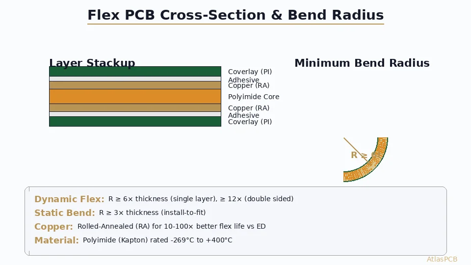
- Temperature range: –269°C to +400°C
- Dielectric constant: 3.2–3.5 at 1 GHz
- Tensile strength: 231 MPa
- Best for: Dynamic flex, high-temperature, aerospace
Polyester (PET) — Cost-Optimized
- Temperature range: –60°C to +105°C
- Lower cost than polyimide (~40% savings)
- Cannot be soldered directly (max 105°C)
- Best for: Static flex in consumer electronics, membrane switches
Liquid Crystal Polymer (LCP) — RF Applications
- Dielectric constant: 2.9 at 10 GHz
- Extremely low moisture absorption (0.04%)
- Best for: 5G mmWave flex antennas, high-frequency interconnects
Copper Types: RA vs. ED
Copper foil selection critically impacts flex life:
| Property | Rolled-Annealed (RA) | Electrodeposited (ED) |
|---|---|---|
| Grain structure | Elongated, parallel | Columnar, perpendicular |
| Flex endurance | 10–100× better | Limited |
| Surface roughness | Low (Rz < 2 µm) | Higher (Rz 3–8 µm) |
| Cost | 1.5–2× more expensive | Standard |
| Min. thickness | 9 µm (¼ oz) | 5 µm (available thinner) |
| Best for | Dynamic flex | Static flex, HDI flex |
Design Rule: Always specify RA copper for any circuit that will experience repeated bending. ED copper is acceptable only for install-to-fit (one-time bend) applications.
Adhesive vs. Adhesiveless Construction
Adhesive-based laminates bond copper to polyimide using acrylic or epoxy adhesive (12–25 µm thick). They are lower cost but add thickness, reduce flexibility, and limit operating temperature to the adhesive’s Tg.
Adhesiveless laminates deposit or laminate copper directly onto polyimide. Benefits include:
- Thinner construction (better bend performance)
- Higher temperature capability
- Better impedance control (no adhesive dielectric uncertainty)
- Required for fine-pitch flex (< 75 µm line/space)
Bend Radius: The Critical Design Parameter
Calculating Minimum Bend Radius
The bend radius determines whether copper will crack under flexing stress. The outer copper surface experiences tensile strain:
Strain = t / (2R + t)
Where:
- t = total circuit thickness at the bend
- R = bend radius (inner surface to neutral axis)
Copper fatigue failure occurs when strain exceeds the endurance limit. IPC-2223 provides conservative guidelines:
Static (install-to-fit, ≤1 cycle):
- Single-layer: R ≥ 3× total thickness
- Double-sided: R ≥ 6× total thickness
- Multilayer: R ≥ 12× total thickness
Dynamic (repeated flexing, >100 cycles):
- Single-layer: R ≥ 6× total thickness
- Double-sided: R ≥ 12× total thickness
- Multilayer: R ≥ 24× total thickness
Reducing Bend Radius When Space Is Tight
When the enclosure demands a tighter bend:
- Reduce copper weight: Drop from 1 oz to ½ oz or ¼ oz in the flex zone
- Use single-sided construction: Eliminates the neutral-axis offset problem
- Stagger traces on dual-access flex: Route conductors only on the tension-neutral side
- Remove coverlay at the bend: Bare copper is thinner (but less protected)
- Use hatched copper planes: Ground planes in flex zones should be hatched (50–70% fill) rather than solid to improve flexibility
- Bookshelf the layers: In multi-layer flex, offset conductors so they don’t stack directly, distributing strain
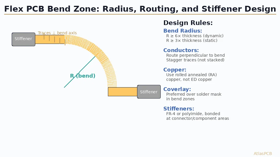
Trace Routing Through Bend Zones
Critical routing rules for the bend area:
- Route perpendicular to the bend axis — traces should cross the bend at 90° to minimize strain
- Never place vias in bend zones — the plated barrel is rigid and cracks
- Transition traces gradually — use smooth curves (teardrops) when entering the flex zone from a rigid area
- Maintain uniform trace distribution — uneven copper density causes localized stress concentrations
- No sharp trace direction changes — use arcs with R ≥ 0.5 mm for any turn in the flex area
Rigid-Flex Stackup Design
Architecture Types
Rigid-flex PCBs combine rigid and flex sections in a single unified structure:
Type 1: Flex layers penetrate entirely through the rigid section
- Flex polyimide layers serve as the substrate for rigid areas too
- Simplest construction, fewest layer transitions
- Best for: 2–4 layer designs with simple connectivity
Type 2: Rigid layers added only in stiffened areas
- Separate FR-4 cap layers are added above/below the flex core in rigid zones
- Allows high layer count (8–20 layers) in rigid sections while keeping flex thin
- Most common architecture for complex designs
Type 3: Multiple flex sections at different stackup positions
- Different flex layers route to different Z-positions
- Enables 3D interconnect geometries
- Most expensive, used in military/aerospace
Transition Zone Design
The rigid-to-flex transition is the highest-stress area and the most common failure point:
- Minimum overlap: Rigid laminate must overlap flex by ≥1.5 mm (preferably 2.5 mm)
- No vias within 0.5 mm of transition: Plated holes near the flex boundary crack from repeated thermal cycling
- Bevel the rigid edge: A 45° chamfer on the FR-4 edge reduces stress concentration
- Anchor pad placement: First component pad should be ≥2 mm from the transition
- Stiffener consideration: Add polyimide or FR-4 stiffeners on the flex side if components mount near the transition
Layer Count Planning
Typical rigid-flex stackups:
| Application | Rigid Layers | Flex Layers | Total |
|---|---|---|---|
| Consumer wearable | 4 | 1–2 | 4–6 |
| Medical implant | 6 | 2 | 6–8 |
| Aerospace avionics | 10–16 | 2–4 | 12–20 |
| Smartphone main board | 8–12 | 1–2 | 8–14 |
Design Rule: Minimize flex layer count. Every additional flex layer doubles minimum bend radius. Route power and ground in the rigid sections and use flex only for essential signal interconnects.
Impedance Control in Flex Circuits
Challenges Unique to Flex
Impedance control in flex circuits faces several complications:
- Polyimide Dk variation: Dk ranges 3.2–3.5 depending on manufacturer, moisture, and construction
- Adhesive layer uncertainty: If using adhesive-based laminate, the adhesive Dk (~3.0–3.5) adds unpredictability
- No soldermask reference: Coverlay doesn’t provide the same controlled dielectric as rigid soldermask
- Thickness tolerance: Flex materials have wider thickness tolerances (±15% vs. ±10% for FR-4)
Achieving Controlled Impedance
For flex circuits requiring impedance control:
- Use adhesiveless laminate: Eliminates one unknown dielectric layer
- Stripline over microstrip: Embed controlled-impedance traces between ground planes for more predictable fields
- Specify Dk tolerance: Request material with ±0.1 Dk tolerance (costs more but essential for RF)
- Ground reference proximity: Keep the ground plane as close as possible to the signal layer (typically 25–50 µm polyimide between signal and ground)
- Coupon testing: Always include impedance test coupons on the flex panel
Typical achievable tolerance: ±10% for flex (vs. ±7% on rigid boards).
Need Rigid-Flex PCB Manufacturing?
AtlasPCB specializes in complex rigid-flex with 1–6 flex layers, controlled impedance, and IPC Class 3 reliability. DFM review included with every order.
Get a Rigid-Flex Quote →Design for Manufacturing: Flex-Specific DFM Rules
Panel Layout
Flex circuits are manufactured on large panels (typically 12” × 18” or 18” × 24”):
- Grain direction: Align the bend axis perpendicular to the copper grain direction (RA copper has a defined grain)
- Fiducials: Add at least 3 fiducials per flex panel for coverlay alignment
- Breakaway tabs: Use 0.3–0.5 mm wide tabs with mouse-bite perforations for singulation
- Fold registration marks: Add targets showing where the circuit will be folded in assembly
- Outline tolerance: ±0.1 mm for laser-cut, ±0.15 mm for die-cut outlines
Pad and Via Design
- Teardrop pads: Mandatory on all pads in or near flex zones — gradual taper prevents crack initiation
- Pad anchoring: Use anchoring spurs (copper extending from pad into trace) to prevent pad lifting
- Button plating: For blind vias in flex, use button-plated (filled) vias to prevent solder wicking
- Via-in-pad: Acceptable in rigid zones only — never place via-in-pad in flex areas
- Annular ring: Minimum 100 µm (larger than rigid standard of 75 µm) to account for registration tolerance
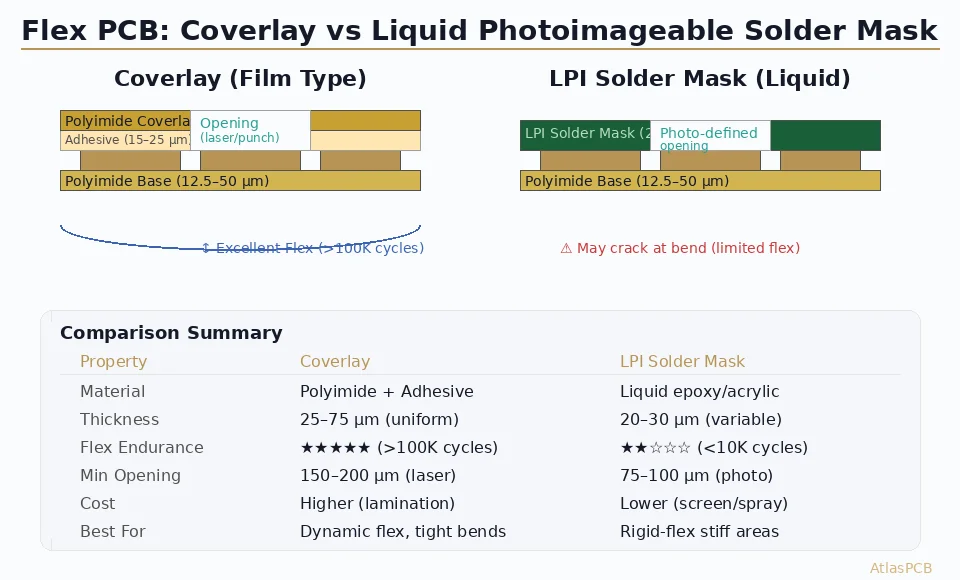
Coverlay Design
Coverlay (polyimide + adhesive film) replaces soldermask on flex circuits:
- Opening tolerance: ±0.1 mm (worse than LDI soldermask ±0.025 mm)
- Minimum bridge: 0.2 mm coverlay web between adjacent openings
- Adhesive squeeze-out: Allow 0.075 mm clearance around openings for adhesive flow
- No coverlay in bend zone: Where coverlay openings cross the bend, ensure exposed copper is protected by conformal coating
Reliability Testing and Qualification
IPC-2223 Test Methods
Qualifying flex and rigid-flex designs requires:
Flex Endurance (IPC-TM-650 2.4.3)
- Mandrel bend test: Flex over a specified radius for N cycles
- Pass criteria: No opens, no resistance increase >10%
- Typical requirement: 100,000 cycles for dynamic flex
Thermal Shock
- –65°C to +125°C, 100–500 cycles
- Verifies transition zone integrity
- Common failure: delamination at rigid-flex interface
Peel Strength (IPC-TM-650 2.4.9)
- Copper-to-polyimide adhesion
- Minimum: 0.7 N/mm after thermal stress
- Critical for adhesiveless constructions
Dimensional Stability
- Measures shrinkage/expansion after etching and lamination
- Critical for fine-pitch flex with ≤50 µm features
Common Failure Modes and Prevention
| Failure Mode | Root Cause | Prevention |
|---|---|---|
| Copper cracking at bend | Radius too tight or ED copper | Increase radius, use RA copper |
| Delamination at transition | Thermal stress, insufficient overlap | Increase overlap to 2.5 mm |
| Pad lifting | No anchors, thin adhesive | Add teardrops + anchoring spurs |
| Coverlay peeling | Poor surface prep, tight openings | Plasma clean, increase clearance |
| Impedance drift | Moisture absorption in polyimide | Bake before assembly, seal edges |
Advanced Flex Technologies
Stretchable Circuits
Beyond bending — circuits that stretch:
- Serpentine trace routing: Horseshoe or zigzag patterns allow 30–50% elongation
- Thermoplastic polyurethane (TPU) substrate: Replaces rigid polyimide
- Applications: Wearable health monitors, soft robotics, e-textiles
- Limitations: Cannot achieve fine pitch (<100 µm), limited layer count (1–2)
High-Frequency Flex
For 5G and mmWave applications:
- LCP substrates: Dk 2.9, Df 0.002 at 77 GHz
- Modified polyimide (MPI): Dk 3.0, Df 0.005 at 10 GHz (lower cost than LCP)
- PTFE-flex hybrids: Rogers materials bonded to flex circuits
- Typical applications: Antenna-in-package (AiP), phased array feeds
Embedded Components in Flex
Integrating passives within the flex stackup:
- Embedded resistors: NiCr thin-film deposited on polyimide
- Embedded capacitors: High-Dk polyimide layers (Dk 10–25)
- Benefits: Reduces assembly height, improves high-frequency performance
- Limitations: Fixed values, limited to small-value passives
Internal Links and Resources
For more on related PCB technologies:
- Learn about via-in-pad design rules for rigid sections of your rigid-flex design
- Explore HDI sequential lamination techniques used in high-layer-count rigid-flex
- Review our impedance control guide for achieving tight tolerance in both rigid and flex sections
- Check PCB delamination causes relevant to rigid-flex transition failures
Further Reading
- IPC-2223C: Sectional Design Standard for Flexible Printed Boards
- DuPont Kapton® Polyimide Film Technical Data
- IPC-6013D: Qualification and Performance Specification for Flexible/Rigid-Flex Printed Boards
Ready to start your flex or rigid-flex PCB project? Request a DFM review from our engineering team — we’ll analyze your stackup, bend radius, and transition design before production begins.
About AtlasPCB — We specialize in complex PCB manufacturing for HDI, RF, and high-reliability applications. Explore our rigid-flex PCB manufacturing, multilayer PCB fabrication up to 30 layers, or get an full PCB manufacturing capabilities . Every order includes free engineering review. Get your quote.
Reviewed by AtlasPCB Engineering Team — IPC-certified manufacturing specialists with 15+ years of production experience in HDI, RF, and high-reliability PCB fabrication. Content based on factory floor data and real customer design reviews.
- flex PCB
- rigid-flex
- bend radius
- polyimide
- IPC-2223
- stackup design
- flexible circuits