· AtlasPCB Engineering · Engineering · 8 min read
How to Order PCB from China: Complete Guide for Engineers
A practical guide to ordering PCBs from China — covering file preparation, manufacturer selection, communication, quality verification, shipping, and common pitfalls to avoid.
China produces over 50% of the world’s PCBs — from simple 2-layer prototypes to 60+ layer HDI boards for leading electronics companies. Ordering from China gives you access to massive manufacturing capacity at competitive prices.
But the process is different from ordering domestically. This guide covers every step — from preparing your files to inspecting the delivered boards.
Step 1: Prepare Your Files
Good files prevent 80% of ordering problems. Incomplete or ambiguous files force the manufacturer to make assumptions — and assumptions cause failures.
Required Files
| File | Format | Content |
|---|---|---|
| Copper layers | Gerber (RS-274X or Gerber X2) | One file per copper layer |
| Solder mask | Gerber | Top and bottom |
| Silkscreen | Gerber | Top (and bottom if used) |
| Paste stencil | Gerber | Top and bottom (for assembly) |
| Board outline | Gerber or DXF | Board edge, cutouts, slots |
| Drill files | Excellon (NC Drill) | Plated holes and non-plated holes as separate files |
| Fab drawing | PDF or Gerber | Dimensions, tolerances, notes |
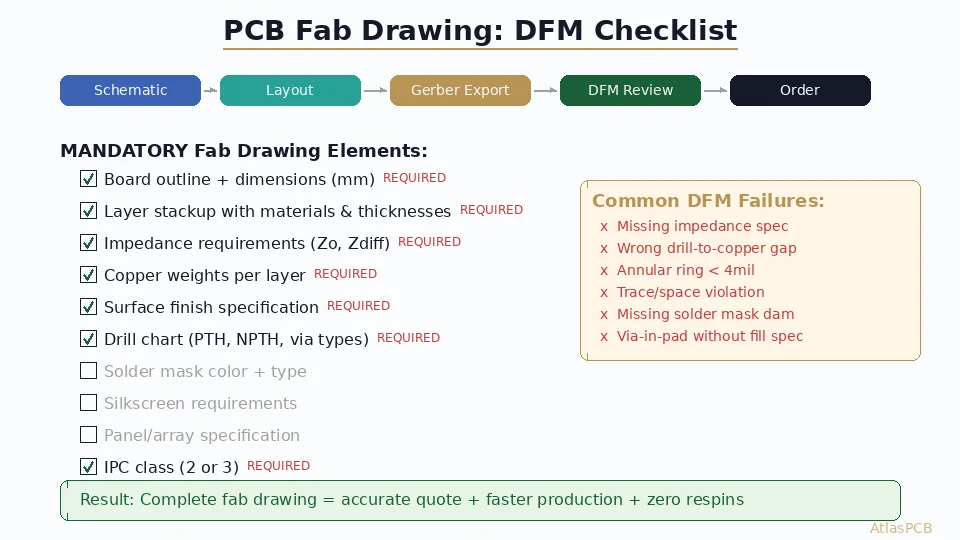
Fab Notes Checklist
Your fab drawing or separate fab notes document must specify:
- Board dimensions with tolerances
- Board thickness (e.g., 1.6mm ±10%)
- Layer count
- Material specification (not just “FR4” — specify grade, Tg)
- Copper weight per layer (e.g., 1oz outer, 0.5oz inner)
- Surface finish (ENIG, HASL, OSP, etc.)
- Solder mask color (green, black, white, etc.)
- Silkscreen color (white, black, yellow)
- Minimum trace width and spacing
- Impedance requirements (target Ω, tolerance, trace type, reference layer)
- IPC class (Class 2 or Class 3)
- Via fill requirements (if applicable)
- Special requirements (back-drill, edge plating, controlled depth, scoring/routing)
File Organization
Package all files in a single ZIP file with a layer mapping document:
project_v1.2.zip
├── README.txt (layer mapping)
├── gerbers/
│   ├── top_copper.gbr
│   ├── inner_2.gbr
│   ├── inner_3.gbr
│   ├── bottom_copper.gbr
│   ├── top_mask.gbr
│   ├── bottom_mask.gbr
│   ├── top_silk.gbr
│   ├── top_paste.gbr
│   └── board_outline.gbr
├── drill/
│   ├── plated.drl
│   └── non_plated.drl
└── fab_drawing.pdf
The README.txt layer mapping prevents errors. Chinese manufacturers process thousands of orders — a clear mapping like “top_copper.gbr = Layer 1 (Top)” eliminates ambiguity.
Step 2: Choose a Manufacturer
The most important decision in the process. See our [guide to choosing a Chinese PCB manufacturer]/blog/complex-pcb-manufacturer-china/) for detailed evaluation criteria.
Quick Selection Framework
| Board Complexity | Manufacturer Tier | Typical Price Range (per board, prototype qty) |
|---|---|---|
| 2-layer FR4 | Any (Tier 2-3) | $2-10 |
| 4-layer FR4 | Tier 2-3 | $15-50 |
| 6-8 layer FR4 | Tier 2 | $40-120 |
| 10-16 layer FR4 | Tier 1-2 | $80-300 |
| HDI (1-N-1) | Tier 1 | $150-500 |
| RF (Rogers) | Tier 1 (RF specialist) | $100-400 |
| 20+ layer | Tier 1 | $200-800+ |
Do not choose solely on price. A $50 saving on prototypes that arrive out of spec costs you $5,000+ in debug time and reorders.

Step 3: Submit and Communicate
Quotation Process
- Submit your files through the manufacturer’s portal or email
- Specify quantity, delivery date requirement, and any special testing
- Receive quotation (typically within 24 hours)
- Review the quotation for accuracy — confirm they understood your layer count, material, finish, and impedance requirements
- Approve and submit PO
Critical Communication Points
After submission, confirm these in writing:
- Stackup confirmation — Ask the manufacturer to return their proposed stackup with material selection and dielectric thicknesses. Compare to your design intent.
- Impedance commitment — Confirm they will calculate impedance on the actual stackup and provide TDR data.
- Material confirmation — For RF boards: confirm the specific laminate and thickness. For high-reliability: confirm material grade and Tg.
- Any design modifications — Explicitly ask: “Will you make any modifications to my design? If so, contact me for approval before proceeding.”
Communication Tips for Working with Chinese Factories
- Be explicit. Do not assume anything is obvious. Write “1oz copper on layers 1 and 8, 0.5oz on layers 2-7” — not “standard copper weight.”
- Use visual references. Annotated screenshots of Gerber viewers are clearer than text descriptions.
- Confirm critical specs in the order acknowledgment. If the acknowledgment does not mention impedance, it may not be tested.
- Keep emails concise. One topic per email. Long emails with multiple questions get partially answered.
- Time zone awareness. China is UTC+8. Expect responses during 9:00-18:00 Beijing time.
Step 4: Monitor Production
For standard orders, monitoring is minimal — the manufacturer produces and ships within the quoted lead time.
For complex or critical orders, request:
- Engineering review confirmation — Notification that files have been reviewed and accepted
- First article photo — Photo of the first board off the line before full production runs
- Impedance test data — Often available before shipping
- Production status updates — Especially for orders with tight deadlines
Step 5: Shipping
Shipping Options
| Method | Transit Time | Cost (10 boards) | Tracking |
|---|---|---|---|
| DHL Express | 3-5 days | $30-60 | Full |
| FedEx Express | 3-5 days | $30-60 | Full |
| UPS Express | 3-5 days | $30-60 | Full |
| Economy (e.g., Yanwen) | 15-25 days | $10-20 | Limited |
| Sea freight | 30-45 days | Cheapest (volume only) | Full |
For prototypes, always use express shipping. The $30-50 cost is insignificant compared to the engineering time waiting for boards.
Customs and Import
- PCBs are classified under HS code 8534.00 (printed circuits)
- Import duty varies by country (US: 0% for bare PCBs from China under certain conditions; check current tariff schedule)
- Declare accurate value — undervaluation causes customs delays
- No special import licenses required for bare PCBs in most countries
- RoHS compliance documentation may be requested by customs in EU
Step 6: Incoming Inspection
When boards arrive, inspect before sending to assembly:
Minimum Inspection (All Orders)
- Visual check — Board appearance, solder mask quality, obvious defects
- Dimensions — Board length, width, thickness (caliper measurement)
- Hole quality — Visual inspection of drill holes (clean, no burrs)
- Quantity — Count matches order (most manufacturers include 1-2 extras)
Standard Inspection (Complex Boards)
- Impedance report review — TDR data matches specification ±tolerance
- Material certificate — Correct laminate grade and lot traceability
- Electrical test report — Continuity and isolation pass for all nets
- Surface finish — Correct type (ENIG gold color, not HASL tin appearance)
Enhanced Inspection (First Order / Critical Boards)
- Cross-section — Send 1 board to a microsection lab. Verify plating thickness, registration, and dielectric thickness.
- Impedance measurement — Independent TDR verification (not just the manufacturer’s data)
- Ionic cleanliness — If Class 3, verify contamination levels
- Functional test — Assemble and test 1 board before committing to full assembly run
Common Pitfalls and How to Avoid Them
| Pitfall | Impact | Prevention |
|---|---|---|
| Incomplete fab notes | Manufacturer makes wrong assumptions | Use the fab notes checklist above |
| Choosing on price alone | Capability mismatch → failed boards | Match manufacturer tier to board complexity |
| Not reviewing stackup | Wrong dielectrics → impedance failure | Request and approve stackup before production |
| No impedance specification | Manufacturer does not control impedance | Explicitly list all impedance requirements in fab notes |
| Material not specified | Cheapest FR4 used regardless of requirements | Specify exact material grade and Tg |
| Not requesting quality docs | Cannot verify quality after delivery | Require TDR, material cert, and e-test with every order |
| Rush prototype on complex board | Engineering shortcuts → quality issues | Allow proper lead time; 2 days saved is not worth a failed prototype |
Using an Intermediary vs. Direct Factory
| Factor | Direct Factory | Intermediary (Atlas PCB) |
|---|---|---|
| Price | Lower (10-20%) | Higher (includes service markup) |
| Engineering review | Varies (may be minimal) | 12-hour human review on every order |
| Communication | In Chinese (or translation) | In English, technical level |
| Material verification | You must verify | Verified by intermediary |
| Factory qualification | You must do it | Already done |
| Problem resolution | You handle directly | Intermediary manages |
| Best for | Simple boards, established relationships | Complex boards, new projects, engineers who need support |
For simple 2-4 layer FR4 boards: Ordering direct from a platform-style manufacturer is fine. The risk is low and the cost savings are meaningful at volume.
For complex boards (HDI, RF, high-multilayer, Class 3): An intermediary reduces risk substantially. The engineering review alone often catches issues that would cost more than the service premium.
How Atlas PCB Simplifies China PCB Ordering
Atlas PCB exists specifically for engineers ordering complex boards from China:
- Upload Gerbers — we handle file review, manufacturer selection, and factory communication
- 12-hour engineering review — stackup, impedance, DFM verified before production
- English technical communication — all factory dialogue in Chinese; you get summarized decisions in English
- Material verification — laminate CoC from material manufacturer, not just factory claim
- Quality documentation — impedance report, material cert, e-test data with every shipment
- 1-piece minimum — prototypes get the same process as production
Upload your Gerbers to get started, or talk to an engineer about your project.
Frequently Asked Questions
What files do I need to order a PCB from China?
You need Gerber files for all copper layers, solder mask, silkscreen, paste stencil, and board outline; Excellon drill files with plated and non-plated holes designated separately; and a fab drawing specifying material, copper weight, surface finish, thickness, impedance requirements, and IPC class. Package everything in a single ZIP with a README file that maps each file to its layer. Complete documentation prevents the manufacturer from making assumptions that may not match your design intent.
How long does it take to get PCBs from China?
Simple boards (2-4 layer FR4): 5-7 working days manufacturing + 3-5 days DHL/FedEx shipping = 8-12 days total. Standard multilayer (6-12 layers): 8-15 working days + shipping. Complex boards (HDI, RF, 16+ layers): 12-20 working days + shipping. Add 1-3 days for engineering review at the front end. Economy shipping saves $20-40 but adds 10-20 days — for prototypes, the engineering time cost of waiting far exceeds the shipping savings.
What should I check when I receive PCBs from China?
At minimum: visual inspection, dimension/thickness measurement, and quantity count. For complex boards: review the impedance test report (TDR data vs specification), material certificate (correct laminate), and electrical test report. For first orders from a new manufacturer: cross-section one board to verify plating thickness and registration, and run an independent impedance measurement. These checks take 30-60 minutes and can save weeks of debugging if an issue is caught before assembly.
Related guides: [Complex PCB Manufacturer China]/blog/complex-pcb-manufacturer-china/) | [PCB DFM Checklist]/blog/pcb-dfm-checklist/) | [PCB Manufacturer with Engineering Review]/blog/pcb-manufacturer-engineering-review/)
Further Reading
[HDI PCB Design Guide: Stackup Rules, Via Structures & DFM Checklist]/blog/hdi-pcb-design-guide/)
[PCB Gerber Files: What They Are and How to Generate Them]/blog/pcb-gerber-files-guide/)
[ENEPIG vs ENIG: Which PCB Surface Finish for Your Design?]/blog/enepig-vs-enig/)
[PCB Solder Mask: Types, Colors, and Functions Explained]/blog/pcb-solder-mask-guide/)
[RF PCB Materials Comparison: FR4 vs Rogers vs Taconic vs Isola]/blog/rf-pcb-materials-comparison/)
About AtlasPCB — We specialize in complex PCB manufacturing for HDI, RF, and high-reliability applications. Explore our full PCB manufacturing capabilities . Every order includes free engineering review. Get your quote.
Reviewed by AtlasPCB Engineering Team — IPC-certified manufacturing specialists with 15+ years of production experience in HDI, RF, and high-reliability PCB fabrication. Content based on factory floor data and real customer design reviews.
- order pcb china
- pcb sourcing
- pcb manufacturing
- engineering guide