· AtlasPCB Engineering · Engineering · 8 min read
PCB Fiducial Mark Design: Global vs Local Fiducials for Automated Pick-and-Place Assembly
A comprehensive guide to PCB fiducial mark design, covering global and local fiducial placement rules, IPC-7351B requirements, clearance dimensions, and DFA best practices for high-speed automated SMT assembly.
Why Fiducial Marks Are Critical for SMT Assembly
Every modern PCB that passes through automated Surface Mount Technology (SMT) assembly relies on fiducial marks for machine vision alignment. These small copper reference points allow pick-and-place equipment to calculate the exact position, rotation, and scaling of the board — compensating for panel stretch, registration errors, and mechanical tolerances accumulated during fabrication.
Without properly designed fiducials, placement accuracy degrades rapidly. A 50-micron placement error on a 0.4 mm pitch BGA means solder joints land partially off-pad, causing opens, bridges, or tombstoning after reflow. For modern assemblies with 008004 (0.25 × 0.125 mm) components, even 25 μm of positional uncertainty becomes unacceptable.
This guide covers everything engineers need to know about fiducial mark design — from dimensional standards and placement rules to common mistakes that cause assembly rejects.
Understanding Machine Vision Alignment
Modern pick-and-place systems use downward-looking cameras to locate fiducials before component placement begins. The alignment process works in three stages:
Stage 1 — Global Registration: The machine finds three global fiducials to establish the board’s coordinate system. Two fiducials define the X-axis vector, while the third (offset in Y) resolves rotation and Y-position. This three-point system corrects for:
- X and Y translational offset
- Rotational misalignment (θ)
- Board stretch/shrink (scaling)
Stage 2 — Local Fine-Tuning: For critical components, the machine moves to local fiducials near the component footprint. This secondary correction accounts for localized etching variation and inner-layer registration errors that global alignment cannot resolve.
Stage 3 — Component Centering: After picking a component, the upward-looking camera verifies lead/ball positions on the component itself. The machine combines this with fiducial data to achieve final placement coordinates.
The entire sequence takes milliseconds per component — but its accuracy depends entirely on fiducial quality.
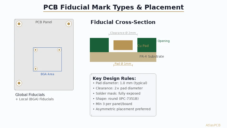
Global Fiducial Design Rules
Global fiducials serve as the board-level reference for the entire assembly program. They establish the master coordinate system that all component placements reference.
Dimensional Standards
| Parameter | Specification | Notes |
|---|---|---|
| Pad diameter | 1.0 mm (±0.05 mm) | Bare copper, no finish variation |
| Clearance zone | 2.0 mm minimum diameter | No copper, mask, or silk |
| Shape | Circular (preferred) | Square/diamond acceptable but less common |
| Copper finish | Flat (HASL, ENIG, OSP) | No solder bump allowed |
| Surface | Exposed copper or final finish | Must not be covered by solder mask |
Placement Rules
The three global fiducials must form an asymmetric pattern — never equilateral or symmetric. This asymmetry allows the vision system to determine board orientation unambiguously:
- Two fiducials along the longest edge — typically the conveyor-parallel edge
- One fiducial at the diagonal opposite corner — creating an L-pattern
- Minimum 5 mm from board edge — keeps fiducials away from panel break-out tabs
- Maximum distance apart — larger triangles improve angular resolution
A common layout places fiducials at three corners of the PCB, leaving one corner empty. This guarantees the vision system can distinguish between top-side-up and bottom-side-up orientation.
What NOT to Do
- Don’t place fiducials symmetrically — the machine cannot determine board rotation
- Don’t use via-in-pad near fiducials — drill remnants confuse pattern recognition
- Don’t place fiducials under stiffeners or labels — optical access is mandatory
- Don’t mix fiducial shapes — all global fiducials should be identical circles
Local (Component-Level) Fiducials
Local fiducials provide fine-alignment correction for individual high-precision components. They are mandatory for:
- BGA packages with pitch ≤ 0.5 mm
- QFP packages with pitch ≤ 0.4 mm
- Connectors with press-fit pins requiring ±50 μm tolerance
- Any component where global alignment alone cannot guarantee pad registration
Design Requirements
Local fiducials are smaller than global fiducials to fit within the component keepout area:
| Parameter | Specification |
|---|---|
| Pad diameter | 0.5–1.0 mm |
| Clearance zone | 1.0–2.0 mm diameter |
| Quantity | 2 per component (diagonal corners) |
| Position | Within 5 mm of component outline |
The two local fiducials should be placed at diagonally opposite corners of the component footprint. This diagonal arrangement provides both X-Y translation and rotation correction specific to that component’s local area.
BGA Fiducial Placement Example
For a 35×35 mm BGA with 0.8 mm pitch (1156 balls):
- Place fiducial #1 at top-left corner, 2 mm from BGA pad boundary
- Place fiducial #2 at bottom-right corner, 2 mm from BGA pad boundary
- Keep clearance zones free of copper pour and stitching vias

Need DFA-Optimized PCB Manufacturing?
Our engineering team reviews fiducial placement, stencil compatibility, and assembly panelization before production begins.
Get a Free DFM Review →Panel-Level Fiducials
When multiple PCBs are fabricated on a shared panel, panel fiducials serve the same role as global fiducials but at the panel level. They are essential for:
- Stencil printer alignment (solder paste application)
- Automated optical inspection (AOI) registration
- Depaneling machine alignment (V-score or tab routing)
Panel Fiducial Rules
- Place 3 fiducials in the panel rail (frame area), following the same L-pattern asymmetry
- Panel fiducials should be larger: 1.5–2.0 mm diameter for robustness
- Maintain ≥10 mm from panel tooling holes
- If the panel uses both top and bottom SMT assembly, place fiducials on both sides
Individual boards within the panel still need their own global fiducials for secondary alignment after depaneling.
Fiducial Mark Materials and Surface Finish
The optical properties of fiducial marks directly affect vision system performance:
Recommended Finishes
| Finish | Contrast | Reflectivity | Suitability |
|---|---|---|---|
| Bare copper + OSP | Excellent | Low (matte) | Ideal — consistent contrast |
| ENIG | Very good | Medium | Flat, uniform gold surface |
| Immersion tin | Good | Low | Acceptable but may darken over time |
| HASL (lead-free) | Poor | High & uneven | Avoid — solder dome creates height variation |
The key requirement is flat, uniform reflectivity across the fiducial surface. HASL creates an unpredictable solder meniscus that varies from board to board, confusing vision systems. If your board uses HASL for economic reasons, consider specifying OSP or ENIG selectively on fiducial pads only — this is a selective surface finish technique that many fabricators support.
Background Contrast
The clearance zone (solder-mask-free area) around the fiducial creates the contrast boundary that vision algorithms detect. For maximum contrast:
- Dark solder mask + bright copper = good contrast
- Green or black mask works best with bare copper fiducials
- White mask may require adjustment of vision lighting parameters
- The FR-4 laminate color in the clearance zone should be consistent
Common Fiducial Design Mistakes
Mistake #1: Fiducials Covered by Solder Mask
Problem: The solder mask opening was accidentally omitted, covering the copper pad.
Fix: Explicitly add the fiducial to your solder mask (paste mask) layer in the Gerber output. Many CAD tools require manual addition to the mask layer if fiducials are created as standalone pads rather than library components.
Mistake #2: Via Within Clearance Zone
Problem: A via or trace runs through the fiducial clearance area, creating an unexpected feature the vision system misidentifies.
Fix: Add a keepout zone (DRC rule) of ≥2× fiducial diameter around each fiducial, applied to all copper layers.
Mistake #3: Inconsistent Sizes Across Panels
Problem: Different board designs on the same panel have different fiducial dimensions, requiring machine re-teaching between boards.
Fix: Standardize all fiducials to 1.0 mm pad / 2.0 mm clearance across your entire product family. Document this in your DFM specification.
Mistake #4: Fiducials on Flex Zones
Problem: On rigid-flex boards, fiducials placed in flex regions distort when the flex bends during handling.
Fix: Always place fiducials in rigid zones. For boards assembled while flat, this is automatic — but verify that assembly handling won’t flex the fiducial region.
IPC Standards for Fiducials
The primary reference standards for fiducial marks are:
- IPC-7351B — Land pattern design (defines fiducial geometry)
- IPC-2221B — Generic PCB design standard (fiducial placement)
- IPC-2615 — Printed board dimensions and tolerances (panel fiducials)
- SMEMA/IPC-HERMES — Equipment communication standard (how machines communicate fiducial data)
IPC-7351B specifies that fiducials should be “solid circles of exposed copper, with a clear area of soldermask that contrasts with the copper.” The standard recommends a 1:2 ratio between pad diameter and clearance diameter.
Practical Implementation in EDA Tools
Altium Designer
Create a dedicated Fiducial_1mm footprint with:
- Top copper layer: 1.0 mm round pad
- Top solder mask: 2.0 mm round opening
- Courtyard: 3.0 mm diameter (keepout)
- Assembly layer: cross-hair for visual identification
KiCad
Use the built-in Fiducial_1mm_Mask2mm footprint from the standard library, or create a custom footprint with the mask expansion set to 0.5 mm per side.
Cadence Allegro
Define fiducials as padstack entries with mask oversize = 0.5 mm. Place them on the “Fiducial” layer and include them in your IPC-2581 output package.
Design Checklist for Manufacturing
Before releasing your PCB design for fabrication:
- Three global fiducials in asymmetric L-pattern
- Local fiducials for all BGAs with pitch ≤0.5 mm
- Local fiducials for all QFPs with pitch ≤0.4 mm
- All fiducials have 2.0 mm mask clearance
- No copper, vias, or silk within clearance zones
- Fiducials placed ≥5 mm from board edges
- Panel rails include 3 additional panel fiducials
- Same fiducial dimensions used across all boards in panel
- Fiducials appear in paste mask layer (if using selective finish)
- Fiducial positions documented in assembly drawing
Conclusion
Fiducial marks are small features with outsized impact on assembly yield. A well-designed fiducial system ensures your pick-and-place equipment achieves its specified placement accuracy — typically ±25 μm at 3σ for modern machines. Conversely, poorly designed or missing fiducials force manual alignment, reduce throughput, and introduce placement errors that cascade into soldering defects.
The investment is minimal: each fiducial occupies approximately 3 mm² of board space. The return is measured in thousands of correctly placed components per hour.
Ready to optimize your PCB for automated assembly? AtlasPCB provides free DFM review including fiducial placement verification, stencil design audit, and panelization optimization. Request a quote →
Further Reading:
About AtlasPCB — We specialize in complex PCB manufacturing for HDI, RF, and high-reliability applications. Explore our PCB assembly services, or get an full PCB manufacturing capabilities . Every order includes free engineering review. Get your quote.
Reviewed by AtlasPCB Engineering Team — IPC-certified manufacturing specialists with 15+ years of production experience in HDI, RF, and high-reliability PCB fabrication. Content based on factory floor data and real customer design reviews.
- PCB design
- fiducial marks
- DFA
- pick-and-place
- SMT assembly
- IPC-7351B
- automated assembly