· AtlasPCB Engineering · Engineering · 9 min read
Direct Metallization for PCB Manufacturing: Carbon, Graphite, and Conductive Polymer Processes Explained
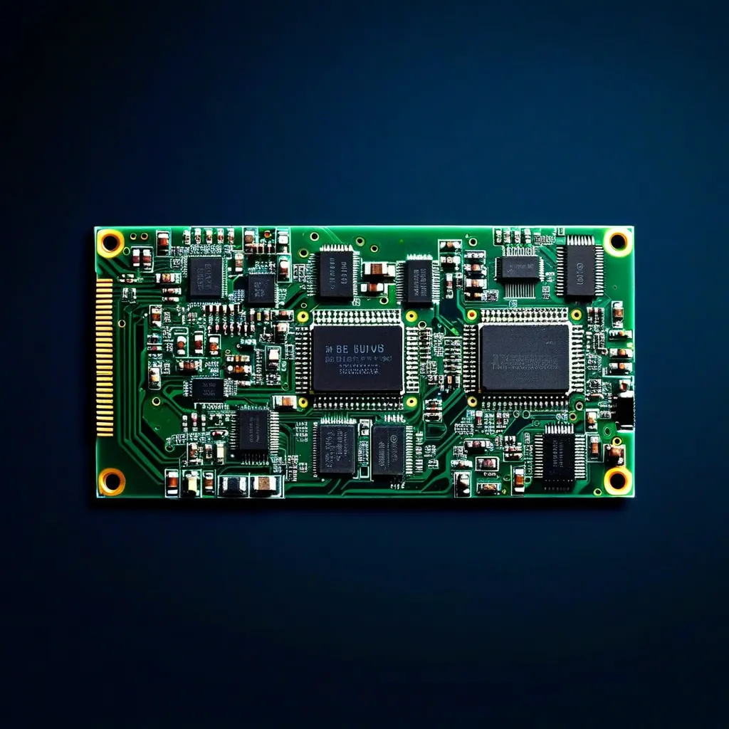
A comprehensive guide to direct metallization technologies that replace electroless copper in PCB via formation — comparing carbon, graphite, and conductive polymer methods for HDI production.
What Is Direct Metallization and Why It Matters
Direct metallization represents a fundamental shift in how PCB manufacturers prepare drilled holes for copper plating. For decades, the industry relied exclusively on electroless copper deposition — a multi-step chemical process requiring palladium catalysts and formaldehyde — to create a thin conductive seed layer on non-conductive via hole walls. Direct metallization achieves the same objective through an entirely different mechanism: applying carbon, graphite, or conductive polymer coatings directly to the hole wall surface.
The significance of this technology has grown substantially as HDI PCB complexity increases and environmental regulations tighten. Applications spanning AI infrastructure, high-performance computing, electric vehicles, and next-generation consumer electronics demand higher interconnect density while fabricators navigate supply chain volatility, sustainability mandates, and cost constraints.
According to a May 2026 technical article published by MacDermid Alpha Electronics Solutions in I-Connect007, direct metallization is now recognized “not just as an alternative process, but as a strategic enabler for future-ready PCB manufacturing.” This assessment reflects growing industry consensus that the technology’s advantages extend well beyond simple process substitution.
How Traditional Electroless Copper Works
Before understanding direct metallization’s advantages, it helps to review the conventional process it replaces.
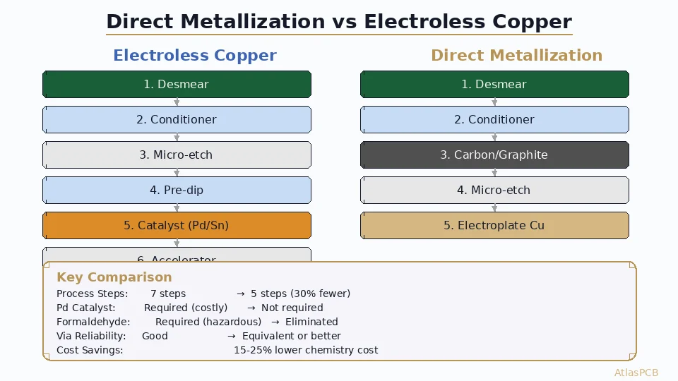
Electroless copper plating follows a seven-step sequence:
- Desmear — Remove resin smear from drilled hole walls using permanganate or plasma
- Conditioner — Prepare the surface for catalyst adsorption
- Micro-etch — Create surface roughness for adhesion
- Pre-dip — Stabilize the catalyst bath
- Catalyst (Pd/Sn) — Deposit palladium-tin colloidal particles that serve as nucleation sites
- Accelerator — Remove tin from the Pd/Sn complex, exposing active palladium
- Electroless copper — Chemically reduce copper ions onto palladium sites using formaldehyde as the reducing agent
This process works well but carries inherent challenges. The palladium catalyst is expensive and subject to price volatility. Formaldehyde is a known carcinogen requiring strict workplace controls. The process generates significant waste streams containing heavy metals. Bath stability requires constant monitoring, and the thin copper deposit (typically 0.3–1.0 μm) can exhibit adhesion issues on certain dielectric materials.
Direct Metallization: Three Technology Variants
Carbon-Based Direct Metallization
Carbon-based systems (such as MacDermid Alpha’s Shadow® process) work by depositing a thin layer of colloidal carbon particles onto the via hole wall. The carbon creates a conductive path with sheet resistance low enough to support subsequent electrolytic copper plating.
Process steps:
- Desmear (permanganate or plasma)
- Conditioner (cationic surfactant prepares surface)
- Carbon/graphite application (colloidal suspension)
- Micro-etch (removes carbon from copper surfaces, retains on dielectric)
- Direct electroplating
The micro-etch step is critical — it selectively removes carbon from horizontal copper surfaces while leaving the coating intact on dielectric hole walls. This selectivity is what makes the process work without shorting adjacent layers.
Graphite Direct Metallization
Graphite-based systems operate similarly to carbon but use crystalline graphite particles that offer slightly higher conductivity. The graphite particles align along the via wall, creating a continuous conductive path. Major suppliers include Atotech (now MKS Instruments) with their neoGanth® product line.
Key advantages of graphite over amorphous carbon include:
- Higher inherent conductivity (lower initial resistance)
- More uniform coverage in high-aspect-ratio holes
- Better bath stability and longer bath life
Conductive Polymer Direct Metallization
Conductive polymer systems deposit polymerized coatings (typically polypyrrole or polyaniline derivatives) onto via walls through oxidative polymerization. These polymers offer the highest conductivity of the three direct metallization variants and excellent adhesion to most dielectric materials.
The process chemistry is more complex than carbon/graphite systems but offers superior throwing power in deep holes, making it suitable for through-holes with aspect ratios up to 12:1.
Performance Comparison: Direct Metallization vs. Electroless Copper
| Parameter | Electroless Copper | Direct Metallization |
|---|---|---|
| Process steps | 7 | 5 |
| Cycle time | 45–60 min | 25–35 min |
| Palladium required | Yes (expensive) | No |
| Formaldehyde | Required (hazardous) | Eliminated |
| Water consumption | Baseline | 30–40% lower |
| Chemistry cost | Baseline | 15–25% lower |
| Max aspect ratio | >15:1 | 8–12:1 (type dependent) |
| Blind microvia coverage | Excellent | Excellent |
| Thermal shock (IST) | Pass IPC-TM-650 | Pass IPC-TM-650 |
| Copper adhesion (peel) | 0.8–1.2 N/mm | 0.7–1.1 N/mm |
The data shows that for the vast majority of HDI applications — where aspect ratios are typically below 8:1 for blind microvias — direct metallization is fully equivalent in reliability while offering significant process and cost advantages.
When to Choose Direct Metallization
Direct metallization excels in these scenarios:
Ideal applications:
- HDI boards with blind and buried microvias (aspect ratio <8:1)
- High-volume production where cycle time reduction compounds
- Facilities targeting environmental compliance improvements
- Any-layer HDI boards for mobile devices and SiP modules
- Facilities reducing hazardous chemical inventories
Where electroless copper remains preferred:
- Very high aspect ratio through-holes (>12:1)
- Thick multilayer boards (>3.2 mm with mechanical drilling)
- Applications requiring extremely uniform seed layers across demanding geometries
- Legacy processes where requalification costs outweigh savings
Need HDI PCBs with Advanced Via Formation?
AtlasPCB operates both direct metallization and electroless copper lines — we select the optimal process for your design requirements.
Get a Free QuoteEnvironmental and Regulatory Drivers
The push toward direct metallization isn’t purely economic. Regulatory pressure is accelerating adoption:
Formaldehyde elimination: The EU’s REACH regulation increasingly restricts formaldehyde use in industrial processes. Direct metallization eliminates it entirely from the metallization step, removing a significant compliance burden.
Palladium supply concerns: Palladium prices have fluctuated between $1,200 and $3,000 per ounce over the past five years. Direct metallization removes this supply chain vulnerability entirely.
Water reduction: With many regions implementing stricter industrial water discharge limits, the 30–40% reduction in water consumption represents a meaningful operational advantage.
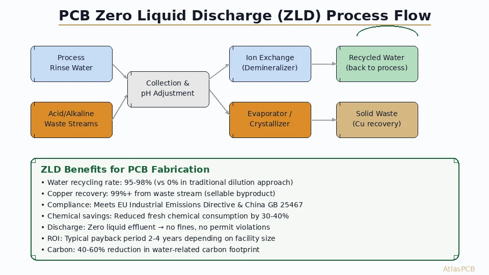
Zero liquid discharge compatibility: Direct metallization generates simpler waste streams that integrate more easily with ZLD systems, reducing the complexity and cost of water treatment infrastructure.
Implementation Considerations
Transitioning from electroless copper to direct metallization requires careful planning:
Equipment modifications
- Replace catalyst and electroless copper tanks with carbon/graphite application tanks
- Upgrade filtration systems (carbon particles require different filter specifications)
- Modify rinse staging (fewer rinse steps needed)
- Update process control systems and monitoring parameters
Qualification testing
- IPC-TM-650, Method 2.6.8 (thermal shock/interconnect stress testing)
- Cross-sectional analysis of via wall coverage
- Pull force testing per IPC-TM-650, Method 2.4.39
- Accelerated aging and solder float testing
Production ramp
- Start with simpler designs (4–8 layer boards with standard vias)
- Progress to HDI with blind microvias after initial qualification
- Maintain electroless copper capability for high-aspect-ratio products during transition
Process Chemistry Deep Dive: Carbon Systems
Understanding the chemistry clarifies why carbon-based direct metallization works so reliably.
Surface preparation
After desmear (either permanganate or plasma), the via wall presents a micro-roughened dielectric surface. The conditioner step deposits a cationic charge on this surface, creating electrostatic attraction for the negatively charged carbon particles.
Carbon application
The carbon bath is a colloidal suspension of sub-micron carbon particles (typically 50–200 nm diameter) in an alkaline aqueous medium. The particles deposit through a combination of electrostatic attraction and Brownian motion, forming a continuous conductive layer approximately 100–200 nm thick.
Sheet resistance of the deposited carbon layer: 1,000–5,000 Ω/square — orders of magnitude higher than metallic copper, but sufficient to support electrolytic plating initiation when combined with appropriate plating bath chemistry and current density.
Selective micro-etch
The critical selectivity step uses a standard micro-etch solution (sodium persulfate or sulfuric-peroxide) that rapidly attacks the thin carbon layer on exposed copper surfaces while leaving it intact on non-conductive via walls. This selectivity works because:
- Carbon-on-copper has weak adhesion (removed in seconds)
- Carbon-on-dielectric has strong adhesion (survives the etch time)
- Process window is wide (typically 30–90 seconds at room temperature)
Direct electroplating
With conductive carbon on the via walls, standard acid copper electroplating can proceed directly. Initial plating at lower current density (0.5–1.5 ASD for the first 2–5 minutes) ensures uniform nucleation on the high-resistance carbon surface before ramping to normal plating conditions.
Quality Assurance and Testing
Qualifying direct metallization requires rigorous testing:
Interconnect Stress Testing (IST)
Per IPC-TM-650, Method 2.6.26, IST applies thermal cycling through resistive heating of the specimen. Direct metallization specimens must survive a minimum of 500 cycles without resistance increase >10%. Production data from multiple fabricators shows typical first failure at 800+ cycles — exceeding electroless copper baseline performance.
Solder float testing
Specimen floated on molten solder at 288°C for 10 seconds (IPC-TM-650, 2.4.13). Direct metallization consistently passes with no delamination or barrel cracking — the absence of the thin electroless copper interlayer actually improves thermal stress distribution.
Backlight testing
100% inspection of drilled panels under transmitted light after carbon application verifies complete coverage. Any pinholes or bare spots appear as bright points. Coverage targets: >98% of hole wall area.
Cross-sectional analysis
Microsectioning per IPC-TM-650, 2.1.1 reveals the carbon layer morphology, subsequent copper adherence, and overall via structure. Key measurements:
- Carbon layer continuity (no bare dielectric spots)
- Copper-to-dielectric adhesion at via knee
- Fill uniformity in blind microvias
- Absence of voiding at interface
Troubleshooting Common Issues
Incomplete coverage (skip plating)
Root cause: Insufficient conditioning, depleted carbon bath, or excessive micro-etch Solution: Verify conditioner concentration and contact time; replenish carbon bath particles; reduce micro-etch time by 10–15 seconds
Copper peeling from via wall
Root cause: Contamination between carbon application and plating; excessive drying of carbon layer Solution: Minimize time between carbon application and plating entry; maintain panel moisture during transfer
Uneven plating distribution in via
Root cause: Carbon layer resistance non-uniformity; inadequate initial plating current Solution: Verify carbon bath agitation and panel dwell time; increase initial “soft start” plating duration
Industry Adoption Status (2026)
Direct metallization has moved well beyond experimental status. Major PCB fabricators across Asia, Europe, and North America have adopted the technology for mainstream production. The technology is particularly dominant in:
- Mobile device HDI boards (smartphone main boards)
- Automotive HDI for ADAS systems
- Any-layer HDI for SiP modules
- High-volume consumer electronics
Industry estimates suggest that direct metallization now accounts for 35–40% of all primary metallization globally, up from approximately 20% in 2020. The growth trajectory indicates that it will become the majority process for HDI applications within the next 3–5 years.
Practical Design Implications for Engineers
For PCB designers, the choice between direct metallization and electroless copper is typically made by the fabricator based on design parameters. However, understanding the technology helps in DFM optimization:
Aspect ratio awareness: If your design requires through-hole vias with aspect ratios above 10:1, discuss metallization approach with your fabricator during early design review.
Microvia design: For blind microvias with typical HDI aspect ratios (0.6:1 to 1:1), direct metallization is fully qualified and offers no design constraints.
Material compatibility: Direct metallization works well with standard FR-4, high-Tg materials, and most low-loss laminates. Some specialty materials may require process optimization.
Cost implications: For high-volume HDI production, direct metallization’s lower per-panel cost can meaningfully impact project economics.
Further Reading
- HDI Microvia: Stacked vs Staggered Reliability
- PCB Copper Plating: Electroless vs Electrolytic for HDI Vias
- Sequential Lamination vs Build-Up HDI Process
- PCB Plasma Desmear Process
Ready to discuss metallization options for your next HDI project? Our engineering team evaluates each design to recommend the optimal via formation process. Request a quote or explore our HDI capabilities.
About AtlasPCB — We specialize in complex PCB manufacturing for HDI, RF, and high-reliability applications. Explore our HDI PCB manufacturing capabilities, or get an full PCB manufacturing capabilities . Every order includes free engineering review. Get your quote.
Reviewed by AtlasPCB Engineering Team — IPC-certified manufacturing specialists with 15+ years of production experience in HDI, RF, and high-reliability PCB fabrication. Content based on factory floor data and real customer design reviews.
- direct metallization
- electroless copper
- HDI PCB
- via formation
- carbon process
- conductive polymer
- PCB manufacturing
- sustainability