· AtlasPCB Engineering · Engineering · 8 min read
Zero Liquid Discharge in PCB Manufacturing: Wastewater Treatment, Copper Recovery, and Sustainability
How modern PCB fabricators achieve zero liquid discharge through ion exchange, evaporation, and crystallization — eliminating wastewater while recovering valuable metals.
From Dilution to Zero Discharge: A Manufacturing Revolution
The PCB industry’s relationship with water has undergone a dramatic transformation. In the early decades of circuit board production, the prevailing philosophy was simple: dilution is the solution. Fabricators used massive volumes of fresh water to dilute contaminants below regulatory limits before discharge. Some facilities consumed 500–1,000 liters of water per square meter of PCB produced.
That era is ending. Driven by tightening discharge regulations, rising water costs, and genuine sustainability commitments, leading PCB manufacturers are implementing zero liquid discharge (ZLD) systems that recycle virtually all process water while recovering dissolved metals as valuable byproducts.
A recent I-Connect007 article chronicling this transition notes that the journey “demonstrates that in the early days of PCB production, prevailing practices revolved around a ‘dilution is the solution’ mentality.” Today’s reality is fundamentally different — ZLD technology has matured to the point where it makes both environmental and economic sense.
Why PCB Manufacturing Generates So Much Wastewater
PCB fabrication is inherently chemistry-intensive. A typical multilayer board passes through dozens of wet process steps:
- Electroless/electrolytic copper plating — acid copper baths, rinse stages
- Etching — acidic or alkaline copper removal (cupric chloride, ammoniacal)
- Developing — photoresist/solder mask development (sodium carbonate, TMAH)
- Stripping — resist removal (sodium hydroxide)
- Surface finishing — ENIG, ENEPIG, immersion tin (multiple chemistry baths)
- Cleaning — degreasing, micro-etching, oxide treatment
Each process step requires multiple rinse stages to prevent cross-contamination. A conventional fabrication facility producing 10,000 m² of PCB per month may generate 200–500 m³ of wastewater daily.
ZLD System Architecture for PCB Facilities
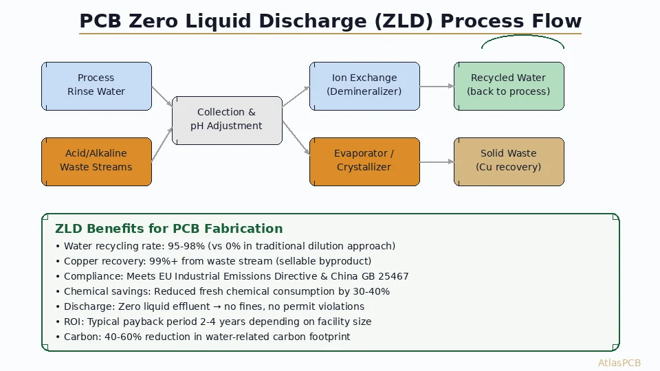
A properly designed ZLD system for PCB manufacturing comprises several treatment stages:
Stage 1: Segregation and Collection
Effective ZLD begins with proper waste stream segregation. PCB facilities typically maintain separate collection systems for:
- Concentrated waste — spent etchant, plating bath dumps (high metal content)
- Acid rinse water — from copper plating, etching rinse stages
- Alkaline rinse water — from developing, stripping, cleaning
- Precious metal waste — from gold, palladium processes
Segregation prevents incompatible chemistries from reacting and ensures each stream receives appropriate treatment.
Stage 2: Primary Treatment (Neutralization and Precipitation)
Mixed acid and alkaline streams are neutralized to pH 7–9, precipitating dissolved metals as hydroxides. Copper, nickel, and tin form insoluble hydroxide sludge that is removed by settling and filtration.
This stage removes 90–95% of dissolved metals but generates a clarified stream that still contains dissolved salts, organics, and trace metals exceeding discharge limits.
Stage 3: Ion Exchange (Demineralization)
Ion exchange columns remove remaining dissolved ions to produce high-purity water suitable for reuse in rinse stages. Modern systems achieve:
- Conductivity reduction from 500–2,000 μS/cm to <10 μS/cm
- Specific copper removal to <0.1 mg/L
- Water recovery rate: 85–90% of input volume
Regeneration waste from ion exchange columns feeds into the evaporator circuit.
Stage 4: Evaporation and Crystallization
The remaining 10–15% concentrate plus ion exchange regenerant enters vacuum evaporation systems. These reduce liquid volume by 90–95% through thermal or mechanical vapor compression evaporation. The distillate returns as ultra-pure water. The remaining concentrate enters a crystallizer that produces solid salt cake for disposal or further processing.
Stage 5: Copper Recovery (Electrowinning)
Concentrated copper streams bypass the general treatment system and enter dedicated electrowinning cells. Copper ions are electroplated onto cathode blanks, producing 99.5%+ pure copper that can be sold. A facility processing 10,000 m² PCB/month typically recovers 500–1,000 kg of copper monthly — a meaningful revenue stream.

Sustainable PCB Manufacturing with Zero Compromise
AtlasPCB's facilities implement advanced water treatment and resource recovery — delivering boards that meet both performance specs and sustainability goals.
Request a QuoteEconomic Analysis: The Business Case for ZLD
Implementing ZLD requires significant capital investment but delivers measurable returns:
Capital costs (medium facility, 5,000–10,000 m²/month)
- Ion exchange system: $80,000–150,000
- Evaporator/crystallizer: $200,000–500,000
- Copper electrowinning: $50,000–120,000
- Piping, controls, building: $100,000–300,000
- Total CAPEX: $500,000–$1.5 million
Annual savings
- Water purchase reduction (90%+): $30,000–80,000
- Discharge fee elimination: $50,000–200,000 (jurisdiction dependent)
- Chemical reduction (30–40%): $40,000–100,000
- Copper recovery revenue: $30,000–80,000
- Regulatory compliance cost avoidance: $20,000–50,000
- Total annual benefit: $170,000–$510,000
Payback period
- Conservative estimate: 3–4 years
- Aggressive (high water cost regions): 1.5–2.5 years
The economics improve dramatically in regions with high water costs (Middle East, parts of Europe) or strict discharge regulations requiring expensive treatment before discharge.
Regulatory Landscape Driving ZLD Adoption
Multiple regulatory frameworks are pushing PCB manufacturers toward zero discharge:
China (GB 25467-2010): China’s PCB effluent standard sets strict limits on copper (<0.5 mg/L), nickel (<0.5 mg/L), and COD (<80 mg/L) in discharge water. Many facilities in Guangdong, Jiangsu, and Hubei provinces face even stricter local requirements, making ZLD economically attractive compared to conventional treatment.
EU Industrial Emissions Directive (IED): The IED requires BAT (Best Available Techniques) for industrial installations, with PCB manufacturing increasingly expected to minimize water consumption and approach zero discharge.
US Clean Water Act / NPDES permits: Individual discharge permits set facility-specific limits that have tightened progressively. Some facilities find ZLD simpler than maintaining increasingly demanding permit compliance.
Technology Selection Guide
Choosing the right ZLD configuration depends on facility size and waste characteristics:
| Facility Size | Recommended Approach | Typical CAPEX |
|---|---|---|
| Small (<2,000 m²/mo) | Ion exchange + concentrate haul-away | $100K–250K |
| Medium (2,000–10,000 m²/mo) | Full ZLD with evaporator | $500K–1.5M |
| Large (>10,000 m²/mo) | Multi-stage ZLD with crystallizer + Cu recovery | $1.5M–4M |
For smaller facilities, a hybrid approach — ion exchange for water recovery plus hauling concentrated waste to a central treatment facility — can provide 85% of ZLD benefits at 30% of full system cost.
Challenges and Limitations
ZLD implementation isn’t without challenges:
Energy consumption: Evaporation is energy-intensive. Modern systems use mechanical vapor compression (MVC) to recover 80–90% of evaporation energy, but electricity costs remain the largest operational expense.
Organic contamination: Photoresist fragments, surfactants, and other organics can foul ion exchange resins and membrane systems, requiring pretreatment.
Scaling and fouling: Calcium and magnesium salts precipitate in evaporators, requiring regular cleaning cycles.
Operator training: ZLD systems require skilled operators who understand water chemistry, ion exchange regeneration, and equipment maintenance.
Space requirements: Full ZLD systems occupy significant floor space — typically 50–200 m² depending on capacity.
Integration with Modern PCB Processes
ZLD systems work synergistically with other process improvements:
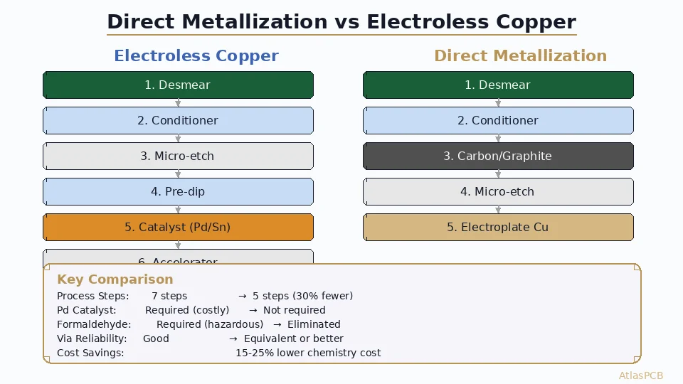
Direct metallization reduces rinse water volume by 30–40% compared to electroless copper, reducing the ZLD system’s processing load.
Closed-loop etchant management recovers copper directly from etchant through electrolysis, keeping concentrated copper out of the general waste stream.
Counter-flow rinsing reduces fresh water demand by cascading rinse water from cleanest to dirtiest stages.
Smart monitoring with IoT sensors enables real-time optimization of rinse water flow rates based on actual contamination levels rather than fixed timers.
Detailed Technology: Ion Exchange for PCB Applications
Ion exchange (IX) is the workhorse of PCB water recycling. Understanding the specifics helps evaluate system proposals:
Resin types for PCB waste
- Strong acid cation (SAC): Removes Cu²⁺, Ni²⁺, Sn²⁺, Fe²⁺/³⁺ — the primary metal contaminants
- Weak acid cation (WAC): Removes hardness (Ca²⁺, Mg²⁺) that causes scaling
- Strong base anion (SBA): Removes SO₄²⁻, Cl⁻, CrO₄²⁻ — anionic contaminants
- Weak base anion (WBA): Removes organic acids and developer chemistry residues
- Chelating resin (iminodiacetic): Selective copper removal from mixed streams — recovers copper specifically for electrowinning
Typical IX train configuration
Feed → WAC → SAC → WBA → SBA → Mixed Bed → Product Water
(pH adjust)                                    (<5 μS/cm)
The mixed bed polisher ensures final water quality meets rinse specifications (typically <10 μS/cm conductivity, equivalent to fresh deionized water).
Regeneration chemistry
SAC resins regenerate with sulfuric acid (5–10%):
- Cu²⁺ on resin + H₂SO₄ → CuSO₄ solution + regenerated resin
- The regenerant effluent (rich in dissolved copper) feeds the electrowinning circuit
SBA resins regenerate with sodium hydroxide (4–6%):
- Regenerant rinse feeds the evaporator circuit
Resin life and replacement
- SAC: 3–5 years (mechanical degradation)
- SBA: 2–4 years (organic fouling reduces capacity)
- Mixed bed: Annual replacement recommended
- Chelating: 5–7 years (expensive but durable)
Advanced Evaporator Technologies
Modern PCB ZLD systems use several evaporation technologies:
Mechanical Vapor Compression (MVC)
The most energy-efficient option for PCB facilities. MVC compresses the steam generated during evaporation, raising its temperature above the boiling point of the feed. This compressed vapor serves as the heat source for continued evaporation — essentially recycling evaporation energy.
- Energy consumption: 20–30 kWh per m³ of distillate
- Capital cost: High ($300K–800K for 5 m³/hour capacity)
- Operational cost: Low (electricity only)
- Concentration factor: 20–50× (reduces volume to 2–5%)
Multi-Effect Evaporator (MEE)
Uses waste heat or steam, with multiple stages at decreasing pressure:
- Energy consumption: 40–80 kWh thermal per m³ (or steam)
- Capital cost: Moderate
- Best for: Facilities with available waste heat or steam
Forced Circulation Crystallizer
The final stage that converts concentrated brine to solid salt cake:
- Operates at boiling point elevation
- Produces >95% dry solids
- Handles super-saturated solutions without fouling
- Required for true zero liquid discharge (not just near-zero)
Monitoring and Control Systems
Modern ZLD operates with extensive instrumentation:
| Parameter | Sensor | Location | Action if OOL |
|---|---|---|---|
| pH | Glass electrode | Feed, IX inlet/outlet | Auto-dose acid/base |
| Conductivity | Inductive | IX product, evaporator feed | Divert or recirculate |
| ORP | Pt electrode | Feed (redox control) | Adjust oxidant dose |
| Cu²⁺ | Colorimetric | IX inlet, electrowinning feed | Valve routing |
| Turbidity | Nephelometric | Clarifier outlet | Recirculate if high |
| Flow | Mag-flow | All process lines | Mass balance tracking |
| Level | Ultrasonic | All tanks | Overflow prevention |
Automated SCADA systems log all parameters, calculate mass balances, and alert operators to deviation conditions before they impact water quality.
Case Study: Sustainability Metrics
A representative ZLD implementation at a medium-scale PCB facility demonstrates:
- Water recycling: 96.5% (from zero prior)
- Copper recovery: 99.2% (780 kg/month recovered)
- Chemical consumption: Reduced 35%
- Carbon footprint: 52% reduction in water-related emissions
- Discharge: Zero liquid effluent since commissioning
- Payback: Achieved in 2.8 years
Further Reading
- PCB Ionic Contamination Testing: SIR and IPC-J-STD-001
- Halogen-Free PCB Materials Guide
- PCB Copper Plating Thickness Uniformity
- PCB Inner Layer Oxide Treatment
Committed to sustainable manufacturing? AtlasPCB integrates advanced water treatment and metal recovery systems across our production facilities. Get a quote for your next project and ask about our sustainability practices.
About AtlasPCB — We specialize in complex PCB manufacturing for HDI, RF, and high-reliability applications. Explore our full PCB manufacturing capabilities . Every order includes free engineering review. Get your quote.
Reviewed by AtlasPCB Engineering Team — IPC-certified manufacturing specialists with 15+ years of production experience in HDI, RF, and high-reliability PCB fabrication. Content based on factory floor data and real customer design reviews.
- zero liquid discharge
- ZLD
- PCB wastewater
- copper recovery
- sustainability
- PCB manufacturing
- environmental compliance
- water treatment