· AtlasPCB Engineering · Engineering · 7 min read
AI-Powered PCB Design Reuse: How Intelligent Automation Is Cutting Layout Time by 60%
Explore how AI-driven design reuse and intelligent automation in EDA tools like Siemens Xpedition are transforming PCB design workflows — reducing routing time, improving DFM compliance, and accelerating time-to-market.

The Productivity Crisis in PCB Engineering
PCB complexity has grown exponentially over the past decade. A modern server board contains 15,000+ components, 50,000+ nets, and requires 20+ signal layers. Yet the engineering workforce hasn’t scaled proportionally. Teams face shorter schedules, stricter DFM requirements, and increasing pressure to achieve first-pass manufacturing success.
The fundamental problem isn’t tool capability — modern EDA platforms are remarkably powerful. The bottleneck is the manual effort required to translate design intent into physical implementation. Engineers still spend 60-70% of their time on repetitive tasks: placing components, routing buses, checking constraints, recreating validated circuits, and assembling documentation.
AI-powered intelligent automation addresses this gap by handling structured, repetitive work while keeping engineers in control of architectural decisions.
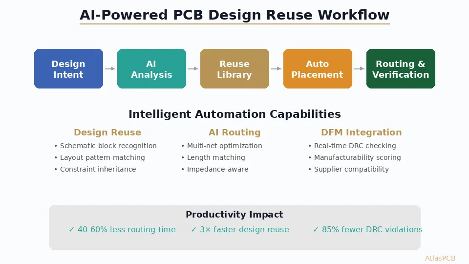
What AI Design Reuse Actually Means
Beyond Simple Block Copy
Traditional design reuse in PCB tools means copying a layout section and pasting it elsewhere. This approach has fundamental limitations:
- Constraints don’t transfer (impedance, spacing, via rules)
- Net names must match exactly or manual remapping is required
- Component value changes break the reuse
- Board outline differences require manual adjustment
- No verification that the reused block still meets its original performance targets
Intelligent Block Recognition
AI-powered reuse, as implemented in tools like Siemens Xpedition, works differently:
- Topology recognition — The AI identifies functional circuit blocks by their schematic topology (e.g., “DDR4 byte lane with termination”), not just by geometric similarity
- Constraint inheritance — When a validated block is recognized, all associated constraints (impedance targets, length matching groups, spacing rules) are automatically inherited
- Adaptive placement — The AI adjusts component positions to fit new board geometry while preserving critical relationships (IC-to-decap distance, differential pair symmetry)
- Variant handling — If a component changes package or value, the AI adapts the layout while maintaining electrical intent
Real-World Impact: DDR Memory Interface Reuse
Consider a DDR5 memory interface — one of the most constraint-intensive sections of any digital board:
Without AI reuse:
- Engineer manually places 200+ components per byte lane
- Manually routes 64+ length-matched signal pairs
- Manually verifies timing margins against DDR5 specification
- Total time per channel: 40-60 hours
With AI-powered reuse:
- AI recognizes DDR5 topology from netlist
- Validated layout block from previous design is adapted
- Length matching and impedance constraints are inherited
- Engineer reviews and adjusts for board-specific constraints
- Total time per channel: 8-15 hours (70-80% reduction)
Intelligent Routing Automation
The Evolution from Auto-Route to AI Route
Early auto-routers (1990s-2010s) used geometric algorithms — they completed connections but produced layouts that experienced engineers would never accept. Routes were inefficient, had unnecessary vias, and violated manufacturing best practices.
Modern AI routing in 2026 uses fundamentally different approaches:
Machine learning trained on expert layouts — AI routing engines learn from thousands of validated designs what “good routing” looks like for different signal types
Physics-aware optimization — Routes are evaluated against electromagnetic simulation models, not just geometric DRC rules
Manufacturing-aware decisions — The AI considers real fabrication constraints (minimum annular ring, acid trap avoidance, etch compensation) during routing, not just after
Multi-objective optimization — Simultaneously optimizes for signal integrity, manufacturing yield, thermal performance, and routability
What AI Routing Does Well (2026 State of Art)
| Task | AI Capability | Human Advantage |
|---|---|---|
| Bus routing (parallel) | Excellent — faster, consistent | None |
| Length matching | Excellent — exact serpentine | None |
| Power distribution | Good — via pattern optimization | Complex island routing |
| Differential pairs | Good — maintains coupling | Novel topology |
| RF matching networks | Limited — needs constraints | Expert tuning |
| Mixed-signal isolation | Moderate — rule-based | Intuition, experience |

Your AI-Optimized Design Needs Manufacturing Excellence
AI-routed boards demand tight manufacturing tolerances. AtlasPCB delivers ±0.5mil trace accuracy and ±7% impedance control for the precision your EDA tools promise.
View Our Capabilities →DFM Integration: The Manufacturing Connection
Real-Time Manufacturability Scoring
Traditional DFM checking happens after layout completion — a sequential process that often requires re-spinning the design. AI-integrated DFM provides continuous feedback during layout:
- Live DRC — Violations highlighted in real-time as routes are placed
- Manufacturability score — A 0-100 score updated continuously based on:
- Minimum feature sizes vs. process capability
- Acid trap risk assessment
- Copper balance per layer
- Via aspect ratio distribution
- Annular ring margins
- Supplier compatibility — AI checks design rules against specific fabricator capabilities from their published specifications
Data Continuity from Design to Manufacturing
One of the most significant AI contributions is maintaining data continuity across the design flow:
Traditional flow (disconnected):
Schematic → (export) → Layout → (export) → Gerber → (email) → Fabricator
                     ↑ manual sync ↑           ↑ data loss ↑
AI-connected flow:
Schematic ↔ Layout ↔ Manufacturing Model ↔ Fabricator
              ↕              ↕                 ↕
         Constraints     DFM Rules      Process Capability
Bidirectional data flow means changes propagate automatically and constraints remain synchronized. The fabricator sees design intent, not just geometry.
Siemens Xpedition: A Case Study in Intelligent Automation
Siemens’ May 2026 blog post on Xpedition highlights their approach to the productivity challenge. Rather than pursuing fully autonomous AI (which replaces the engineer), Xpedition focuses on intelligent automation (which amplifies the engineer):
Key Capabilities
Sketch routing — Engineer draws approximate route paths; AI completes the exact routing with proper clearances, impedance matching, and via placement
Constraint-driven placement — AI suggests component positions based on net connectivity, timing requirements, and thermal constraints
Design reuse library — Validated blocks stored with full constraint context, automatically recognized in new designs
Connected documentation — Manufacturing documentation generated automatically from the living design model, always synchronized
The Productivity Paradox
As Siemens notes, more powerful tools don’t automatically mean more productivity. Each new capability adds complexity for the user. AI’s role is to manage that complexity — handling the implementation details while engineers focus on architectural decisions that require human judgment and experience.
Practical Implementation: Getting Started with AI-Assisted Design
Step 1: Build a Reuse Library
Start capturing validated design blocks with their constraints:
- DDR interfaces (by generation and topology)
- Power supply circuits (by architecture and current)
- Connector fanout patterns (by connector type)
- RF matching networks (by frequency and impedance)
- High-speed SerDes channels (by protocol and data rate)
Step 2: Define Manufacturing Rules Programmatically
Instead of relying on manual DRC rule setup, define manufacturing constraints as data:
- Import fabricator DFM specs as constraint templates
- Version-control your constraint libraries
- Validate constraints against actual manufacturing data
Step 3: Establish Review Workflows
AI doesn’t eliminate review — it makes review more productive:
- Use AI-generated DFM reports as review checklists
- Focus engineering review on architectural decisions, not geometric checking
- Implement continuous integration for PCB designs (auto-check on every save)
Step 4: Measure and Iterate
Track productivity metrics to validate AI tool ROI:
- Time from netlist to first-pass DRC-clean layout
- Number of design re-spins per project
- Manufacturing yield (first-pass vs. rework rate)
- Engineering hours per net (routing productivity)
Impact on PCB Manufacturing
What AI-Designed Boards Mean for Fabricators
As AI routing becomes standard, fabricators see:
Positive changes:
- More consistent designs (fewer amateur layout mistakes)
- Better copper balance (AI optimizes fill patterns)
- More DFM-compliant designs arriving at NPI
- Reduced back-and-forth on design rule violations
New challenges:
- Designs pushing process limits more uniformly (AI finds the optimal boundary)
- More complex stackups (AI enables designs humans wouldn’t attempt)
- Faster design iteration requiring faster quote turnaround
- Need for machine-readable DFM specifications (not just PDF rules)
AtlasPCB’s Position
At AtlasPCB, we publish our manufacturing capabilities in structured formats that AI-enabled EDA tools can consume directly. Our DFM specifications include:
- Minimum feature sizes by layer and process
- Impedance control tolerance by stackup type
- Via filling/plugging capabilities with aspect ratio limits
- Material availability and lead time data
- Process capability indices (Cpk) for critical parameters
This enables AI design tools to validate manufacturability against our actual capabilities during layout — not after.
The Future: What’s Coming in 2027-2028
Generative PCB Design
Current AI assists layout. Next-generation tools will generate layout from specifications:
- Input: Netlist + mechanical constraints + performance targets
- Output: Multiple valid layout options with tradeoff analysis
- Human role: Selection and refinement, not creation
Digital Twin Integration
Real-time connection between design model and manufacturing:
- Design changes automatically update fabrication instructions
- Manufacturing variations feed back to update design margins
- Predictive yield modeling based on actual production data
Collaborative AI Agents
Multiple specialized AI agents working together:
- Placement agent optimizes component positions
- Routing agent completes interconnect
- Thermal agent adjusts copper distribution
- DFM agent validates against fabricator constraints
- All agents negotiate constraints in real-time
Further Reading
- AI-Powered EDA Tools in PCB Design: Autonomous Agents 2026
- IPC-2581 and Digital Twin for PCB Manufacturing
- PCB Design for Testability: DFT and ICT
- Siemens Fuse EDA AI Agent: PCB Workflow Orchestration
Whether you design with AI tools or traditional EDA, manufacturing quality matters. AtlasPCB provides the process consistency and tight tolerances that match the precision of AI-optimized layouts. Get a quote for your next design →
About AtlasPCB — We specialize in complex PCB manufacturing for HDI, RF, and high-reliability applications. Explore our free engineering DFM review . Every order includes free engineering review. Get your quote.
Reviewed by AtlasPCB Engineering Team — IPC-certified manufacturing specialists with 15+ years of production experience in HDI, RF, and high-reliability PCB fabrication. Content based on factory floor data and real customer design reviews.
- AI PCB design
- design reuse
- EDA automation
- Siemens Xpedition
- intelligent routing
- DFM
- PCB workflow