· AtlasPCB Engineering · Engineering · 6 min read
BGA Solder Joint Fatigue: Thermal Cycling Reliability, Coffin-Manson Prediction, and PCB Design Mitigation
Understand how thermal cycling causes BGA solder joint fatigue through creep-fatigue crack propagation. Learn Coffin-Manson lifetime prediction, DNP effects, and PCB design strategies to extend solder joint life.

The Solder Joint Fatigue Problem
Ball Grid Array (BGA) packages dominate modern electronics assembly for their superior I/O density and electrical performance. But every BGA solder joint is a ticking clock: thermal cycling during power-on/off sequences, environmental temperature changes, and localized heating gradually drives fatigue crack propagation until electrical failure occurs.
Understanding solder joint fatigue is critical for any PCB design targeting:
- Automotive (15-year, -40°C to +150°C reliability requirement)
- Industrial (10-year continuous operation with daily cycling)
- Aerospace/Defense (extreme environments, zero-failure tolerance)
- Telecom/Server (24/7 operation with power management cycling)
This article covers the physics of fatigue failure, prediction models, and practical PCB design strategies to maximize joint lifetime.
Physics of Solder Joint Fatigue
CTE Mismatch: The Root Cause
Thermal fatigue originates from the coefficient of thermal expansion (CTE) mismatch between connected materials:
| Material | CTE (ppm/°C) |
|---|---|
| Silicon die | 2.6 |
| BT/bismaleimide substrate | 12–15 |
| FR-4 PCB | 14–17 |
| Ceramic substrate | 6–8 |
| SAC305 solder | 21–23 |
When temperature changes, each material expands or contracts at a different rate. The solder balls, sandwiched between the package substrate and PCB, must accommodate this differential displacement through shear deformation. Over hundreds or thousands of cycles, this cyclic strain drives fatigue damage.
Shear Strain Calculation
The maximum shear strain in a BGA solder ball is approximated by:
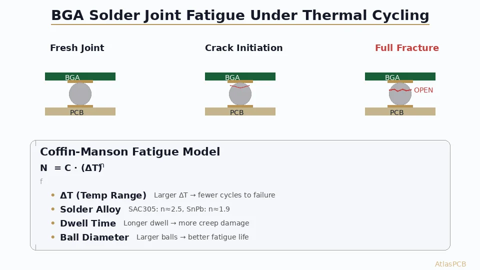
γ = (α_PCB - α_pkg) × ΔT × DNP / h
Where:
- α_PCB, α_pkg = CTE of PCB and package substrate
- ΔT = temperature excursion range
- DNP = Distance from Neutral Point (center of package)
- h = solder ball standoff height
This relationship immediately reveals why corner balls (maximum DNP) fail first, and why larger standoff improves life.
Creep-Fatigue Interaction
Unlike steel or aluminum fatigue (dominated by dislocation-based mechanisms), solder joint fatigue involves coupled creep and fatigue:
During temperature dwells (hold at high/low temperature): Creep deformation occurs as grain boundaries slide under sustained stress. This is time-dependent and stress-driven.
During temperature transitions (ramp up/down): Fatigue-type cyclic strain accumulates. Faster ramps generate less creep but higher instantaneous stress.
Grain coarsening: Over hundreds of cycles, the fine Sn-Ag-Cu microstructure coarsens. Ag₃Sn intermetallic particles agglomerate at grain boundaries, creating preferred crack paths.
Crack propagation: Once initiated (typically at the solder/intermetallic interface), cracks grow incrementally each cycle until the joint resistance increases and eventually opens.
Damage Accumulation Model
The Miner’s rule for linear damage accumulation applies:
D = Σ(1/Nf_i)
Where D = 1.0 represents failure. Each thermal cycle at condition i contributes 1/Nf_i damage, where Nf_i is the cycles-to-failure under condition i alone.
Coffin-Manson Lifetime Prediction
The Modified Coffin-Manson Equation
The industry-standard prediction model for solder joint fatigue life is:
Nf = C × (Δγ)^(-n) × f(dwell) × f(Tmax)
Where:
- Nf = number of cycles to 50% failure (characteristic life)
- C = material constant (depends on solder alloy)
- Δγ = cyclic shear strain range
- n = fatigue exponent (SAC305: 2.0–2.5; SnPb: 1.9–2.1)
- f(dwell) = dwell time correction factor
- f(Tmax) = maximum temperature acceleration factor
Practical Parameters for SAC305
Based on published data from IPC-9701A test programs:
- C ≈ 10–50 (depends on joint geometry and failure criterion)
- n ≈ 2.3 (consensus value for SAC305)
- Dwell correction: Longer dwells reduce life by 15–30% per decade of dwell time increase
- Tmax effect: Every 10°C increase in maximum temperature reduces life by ~20%
Example Calculation
For a 15×15mm BGA on FR-4:
- DNP (corner ball) = 10.6 mm
- Ball diameter = 0.5 mm, standoff h = 0.35 mm
- ΔT = 125°C (-40 to +85°C)
- CTE mismatch = 4 ppm/°C
Shear strain: γ = 4e-6 × 125 × 10.6 / 0.35 = 1.5%
With C=30 and n=2.3: Nf = 30 × (0.015)^(-2.3) ≈ 1100 cycles
This marginal result for automotive (-40 to +125°C target > 1000 cycles) explains why underfill or alternative approaches are needed.
Designing BGAs for Harsh Environments?
AtlasPCB provides IPC-6012 Class 3/3A boards with CTE-optimized stackups, precision pad geometries, and thermal cycling qualification support.
Get Engineering Support →PCB Design Strategies for Improved Fatigue Life
1. Pad Geometry Optimization
Non-Solder-Mask-Defined (NSMD) pads are preferred for fatigue-critical BGAs:
- NSMD pads allow the solder fillet to wrap around the copper pad edge
- This creates a larger solder volume and more compliant joint
- Typical improvement: 20–50% life increase vs SMD pads
Pad size selection:
- Pad diameter should be 80–90% of ball diameter for optimal fillet geometry
- Too small (< 75%): poor wetting, voiding risk
- Too large (> 95%): reduced standoff height, increased strain
2. CTE Management in Stackup
Reduce global CTE mismatch through board construction:
- High-Tg FR-4 (Tg > 170°C): CTE in Z-axis drops above Tg, reducing through-thickness strain
- Low-CTE cores: Aramid-reinforced or ceramic-filled cores reduce XY-plane CTE from 16 to 10–12 ppm/°C
- Balanced copper: Symmetric copper distribution prevents warpage-induced stress concentration
3. Increasing Standoff Height
Design modifications that increase effective standoff:
- Larger ball specification (0.5mm vs 0.3mm balls where pitch allows)
- Controlled paste volume to avoid collapse during reflow
- Non-collapsible balls (with high-Tg core) for critical packages
4. Underfill Application
For automotive/aerospace BGAs:
- Capillary underfill: Post-reflow dispensing, 5–10× life improvement
- No-flow underfill: Pre-applied before placement, simpler process
- Reworkable underfill: Thermoplastic formulations allowing one rework cycle
- Corner staking: Epoxy dots at package corners only—2–3× life improvement with maintained reworkability
5. Local CTE Matching
For extreme-reliability designs:
- Embedded copper coin under large BGAs reduces local PCB CTE
- Metal-core carriers: Copper-Invar-copper constraint layers
- Compliance features: Mechanically decoupled mounting areas
Acceleration Factors for Test Planning
IPC-9701A Test Conditions
| Profile | Tmin | Tmax | ΔT | Dwell | Ramp | Application |
|---|---|---|---|---|---|---|
| TC-A | 0°C | 100°C | 100°C | 10 min | 10°C/min | Consumer/telecom |
| TC-B | -25°C | 100°C | 125°C | 10 min | 10°C/min | Industrial |
| TC-C | -40°C | 125°C | 165°C | 10 min | 10°C/min | Automotive/mil |
| TC-D | -55°C | 125°C | 180°C | 10 min | 11°C/min | Mil/aerospace |
Translating Test Results to Field Life
The acceleration factor (AF) between test and field conditions:
AF = (ΔT_test / ΔT_field)^n × (f_dwell_field / f_dwell_test)
For automotive (field: -40 to +85°C daily, test: -40 to +125°C TC-C): AF ≈ (165/125)^2.3 ≈ 2.0
So 1000 test cycles ≈ 2000 field cycles. At one cycle/day, that’s 5.5 years—insufficient for 15-year automotive targets. This drives the need for design improvements beyond basic BGA assembly.
Failure Analysis Techniques
When solder joints fail in test or field, characterization includes:
- Cross-sectioning: Grind and polish through the joint, image crack path with SEM
- Dye-and-pry: Apply fluorescent dye, separate package, map crack distribution
- X-ray CT: Non-destructive 3D imaging of internal crack morphology
- Daisy-chain monitoring: Real-time resistance measurement during cycling identifies failure location
Typical Failure Modes
- Package-side crack (most common): Crack along the intermetallic compound (IMC) layer at the component pad. Indicates CTE mismatch dominance.
- Board-side crack: Crack at PCB pad interface. Often indicates pad cratering or poor wetting.
- Bulk solder crack: Through the solder ball mid-height. Indicates grain coarsening and thermomechanical fatigue.
- Combined mode: Multiple crack fronts merge. Late-stage failure after extensive cycling.
SAC305 vs. Alternative Solder Alloys
The solder alloy significantly affects fatigue behavior:
| Alloy | Fatigue Exponent (n) | Relative Life | Notes |
|---|---|---|---|
| Sn63Pb37 | 1.9 | 1.0× (baseline) | Legacy, excellent compliance |
| SAC305 | 2.3 | 0.7–1.2× | Industry standard lead-free |
| SAC105 | 2.0 | 1.2–1.5× | More compliant, lower strength |
| Innolot (SAC+Bi+Sb+Ni) | 2.5 | 1.5–2.0× | Highest fatigue resistance |
| SACm (micro-alloyed) | 2.2 | 1.3–1.5× | Drop-in improvement |
For automotive applications, Innolot or SAC+Bi+Sb alloys are increasingly specified for their superior thermal fatigue resistance, despite 10–15°C higher processing temperatures.
Design Checklist for Fatigue-Critical BGAs
- ☐ Calculate DNP and shear strain for corner balls
- ☐ Specify NSMD pads with 80–85% ball diameter ratio
- ☐ Select high-Tg laminate (Tg > 170°C)
- ☐ Ensure symmetric copper balance in stackup
- ☐ Specify underfill or corner staking for automotive/aerospace
- ☐ Include thermal cycling test coupons with daisy-chain BGAs
- ☐ Define acceptance criteria per IPC-9701A (characteristic life)
- ☐ Consider Innolot or micro-alloyed solder for > 1500 cycle targets
Further Reading
- BGA X-Ray Void Analysis per IPC-7095
- BGA Underfill: Capillary, Molded, and Reworkable Options
- CTE Mismatch and Thermal Stress in Multilayer PCBs
- BGA Pad Design and Via-in-Pad Solder Voiding Prevention
Need PCBs that withstand thousands of thermal cycles? AtlasPCB manufactures IPC-6012 Class 3 and Class 3/A boards with controlled CTE stackups, precision BGA pads, and thermal reliability qualification support. Contact our engineering team for fatigue-optimized designs.
About AtlasPCB — We specialize in complex PCB manufacturing for HDI, RF, and high-reliability applications. Explore our HDI PCB manufacturing capabilities, or get an aluminum and metal-core PCB services . Every order includes free engineering review. Get your quote.
Reviewed by AtlasPCB Engineering Team — IPC-certified manufacturing specialists with 15+ years of production experience in HDI, RF, and high-reliability PCB fabrication. Content based on factory floor data and real customer design reviews.
- BGA reliability
- solder fatigue
- thermal cycling
- Coffin-Manson
- SAC305
- creep
- PCB design