· AtlasPCB Engineering · Engineering · 11 min read
Castellated Holes in PCBs: Design Rules, Plating Requirements & Module Applications
Complete guide to castellated hole PCB design covering half-hole plating specifications, design rules for module boards, soldering requirements, and IPC quality standards for castellation.
What Are Castellated Holes?
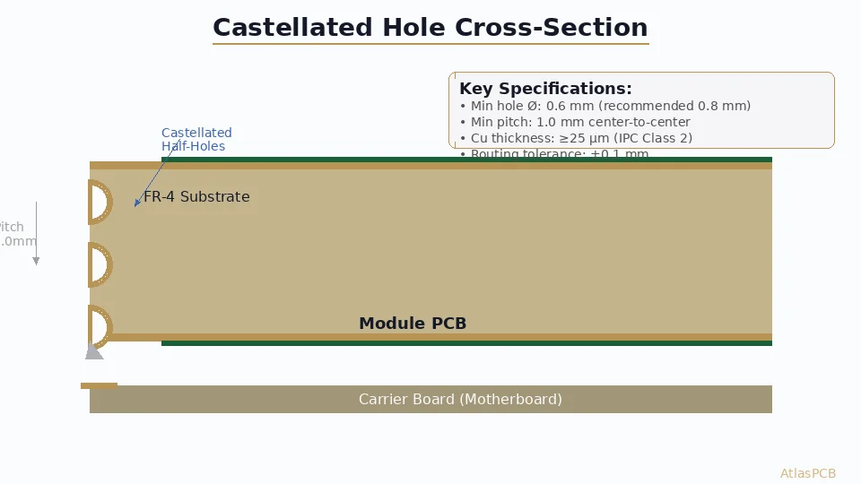
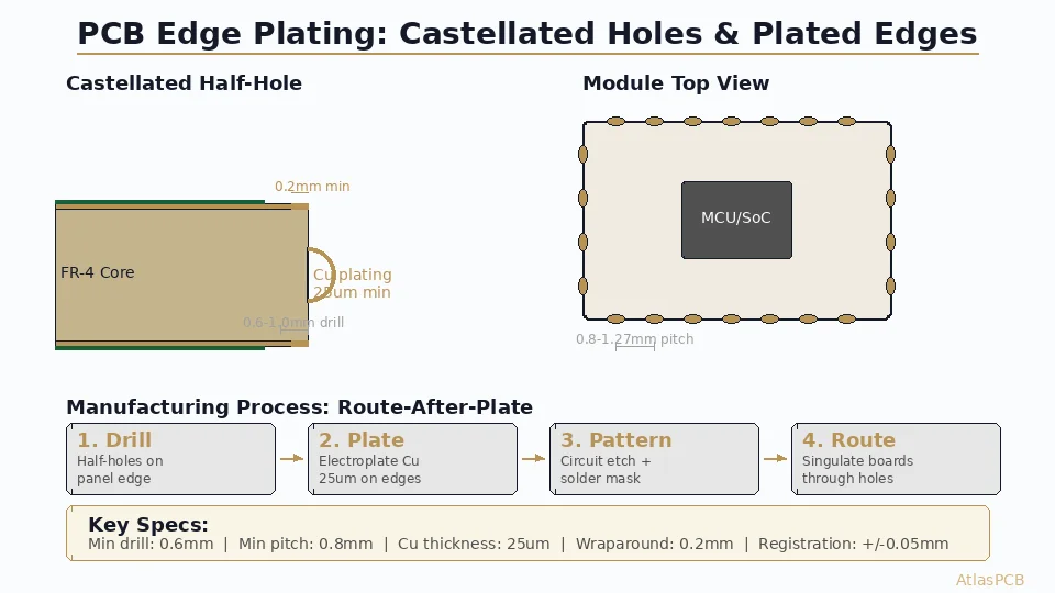
Castellated holes — named after the castle-wall-like appearance they create along a PCB edge — are plated through-holes that are cut in half during board profiling. The result is a series of semicircular, copper-plated indentations along the board edge that serve as soldering contacts.
This elegant design feature enables board-to-board surface mount assembly: a small module PCB with castellated edges can be soldered directly onto a larger host PCB, much like a surface-mount component. The technique eliminates the need for connectors, pin headers, or flex cables, resulting in a compact, low-profile, and highly reliable interconnection.
Common Applications
Castellated holes are ubiquitous in modern electronics:
- Wireless modules: WiFi (ESP32, ESP8266), Bluetooth (nRF52), LoRa, Zigbee modules
- System-on-Module (SoM): Application processor modules, FPGA modules
- Power supply modules: DC-DC converter modules, POL regulators
- Sensor modules: IMU modules, GPS/GNSS modules
- Breakout boards: IC breakout boards for prototyping
- Test fixtures: Modular test adapters
The widespread adoption of castellated modules in IoT, wearables, and embedded systems makes this a critical design skill for modern PCB engineers.
Design Rules for Castellated Holes
Hole Sizing
The drilled hole diameter determines the final castellation size. Since the routing process cuts through the center of the hole, the visible castellation width is approximately half the drilled diameter:
| Drilled Hole Diameter | Castellation Width | Pitch Capability | Process Level |
|---|---|---|---|
| 1.0 mm (40 mil) | ~0.5 mm | ≥1.27 mm | Standard |
| 0.8 mm (31 mil) | ~0.4 mm | ≥1.0 mm | Standard |
| 0.6 mm (24 mil) | ~0.3 mm | ≥0.8 mm | Advanced |
| 0.5 mm (20 mil) | ~0.25 mm | ≥0.65 mm | Premium |
| 0.4 mm (16 mil) | ~0.2 mm | ≥0.5 mm | Ultra-fine |
Recommended minimum: 0.6 mm drilled hole diameter for reliable production. This provides adequate copper surface area for soldering and sufficient mechanical strength.
Pad and Land Design
Module side (castellated board):
- Castellation pad should extend at least 0.25 mm inward from the board edge
- Pad width should be at least 0.15 mm wider than the castellation opening on each side
- Include a thermal relief connection to inner planes if the pad connects to a ground or power pour
- Use the same pad on both top and bottom layers for maximum solder fillet area
Host board side (mother board):
- Landing pad should be at least 1.5× the castellation width
- Pad length (extending from the module footprint edge): 0.5–1.0 mm recommended
- Include solder paste aperture on the landing pads (typically 80–100% of pad area)
- Consider adding thermal relief vias near power/ground castellations for improved thermal performance
Pitch and Spacing
Standard pitch options:
- 2.54 mm (100 mil) — Easy soldering, common for prototyping modules
- 1.27 mm (50 mil) — Standard for commercial wireless modules
- 1.0 mm (40 mil) — Compact modules, requires tighter fabrication control
- 0.8 mm (31 mil) — High-density modules, advanced fabrication required
Minimum spacing between castellations:
- The copper-to-copper gap between adjacent castellation plating must meet the fabricator’s minimum spacing requirement (typically ≥0.15 mm after routing)
- Account for routing tolerance (typically ±0.1 mm) when calculating minimum pitch
Board Edge Clearance
- Castellated holes must be on the routing path — the router bit passes through the center of each hole
- No copper pour should extend to the board edge between castellations (risk of shorts during routing)
- Minimum clearance from castellation hole edge to nearest non-castellation copper: 0.3 mm
- Solder mask should pull back 0.05–0.1 mm from the board edge at castellations to prevent mask chipping
Multi-Row Castellations
For modules requiring more I/O than a single-row edge can provide:
- Two-row castellations are possible but require careful DFM planning
- Inner row holes must be fully plated through-holes (not castellated)
- Stagger the rows for maximum pitch between holes
- Consider whether standard SMD pads on the module bottom might be more practical for the inner connections
For comprehensive DFM guidance on complex hole patterns, see our [DFM checklist]/blog/pcb-dfm-checklist/).
Plating Requirements for Castellations
Copper Plating Thickness
Adequate copper plating is critical for castellation reliability:
- Minimum plating thickness: 25 µm (1 mil) per IPC Class 2
- Recommended plating thickness: 30–35 µm for robust soldering
- IPC Class 3 requirement: 25 µm minimum with 20 µm at any point per IPC-6012
The plating must survive the routing process without delamination. Thicker plating provides:
- Better solder wetting during assembly
- Improved mechanical strength of the half-hole
- Greater resistance to copper burrs during routing
Plating Quality Criteria
After routing, inspect castellation plating for:
- Copper burrs: Small copper fragments remaining at the routed edge — the most common defect
- Delamination: Copper lifting from the hole wall at the cut edge
- Voids: Missing plating in sections of the half-hole
- Roughness: Excessive surface roughness from the routing process
- Concentricity: The router should cut through the exact center of the hole
IPC-6012 acceptability criteria for castellated holes:
- No copper burrs extending beyond the board edge
- No delamination visible at 10× magnification
- Minimum 80% of the half-hole circumference must have continuous plating
- Plating thickness must meet the specified class requirements at any measured point
Surface Finish Considerations
The surface finish on castellated holes affects solderability:
| Surface Finish | Suitability | Notes |
|---|---|---|
| ENIG | Excellent | Gold provides excellent wetting, long shelf life |
| HASL (lead-free) | Good | Adequate for most applications, may have uneven coating in holes |
| OSP | Fair | Short shelf life, may not coat half-hole interior well |
| Immersion Tin | Good | Good solderability, limited shelf life |
| Immersion Silver | Good | Good for fine-pitch castellations |
ENIG is recommended for castellated modules due to its flat surface, excellent solderability, and long shelf life. For more on surface finish selection, see our [surface finish guide]/blog/pcb-surface-finish-guide/).
Manufacturing Process for Castellated Holes
Step-by-Step Process
Drilling: Full plated through-holes are drilled at the designated board edge positions. Holes are drilled on the panel, not at the final board edge — the panel routing will later cut through them.
Electroless copper + Electroplating: Standard PTH plating process deposits copper in the drilled holes. The full-hole geometry at this stage allows for uniform plating — this is a key advantage over trying to plate an already-cut half-hole.
Pattern and etch: Outer layer copper patterns are defined, including the castellation pads.
Solder mask: Applied with pullback from the board edge at castellation locations.
Surface finish: ENIG, HASL, or other finish applied to the castellation pads and hole interiors.
Routing/Profiling: The router bit (typically 1.0–2.0 mm diameter) cuts through the center of each castellated hole, creating the board outline and the half-hole features simultaneously.
Deburring: Post-routing deburring removes copper burrs from the castellated edges. This may include mechanical brushing, chemical etching, or a combination.
Inspection: Visual and dimensional inspection of castellation quality.
Understanding how castellation fits into the overall fabrication flow helps with design optimization. See our [PCB manufacturing process overview]/blog/pcb-manufacturing-process-15-steps/) for the complete production sequence.
Critical Manufacturing Considerations
Router bit selection:
- The router bit diameter must be smaller than the spacing between adjacent castellated holes
- Typical router bit: 1.0 mm or 1.6 mm diameter
- Smaller bits are needed for fine-pitch castellations but wear faster
Routing direction:
- Climb milling (router moves in the same direction as cutting edge rotation) produces cleaner castellation edges
- Some fabricators use a two-pass routing strategy: rough cut + finishing pass
Panel design:
- Castellated boards are typically panelized with the castellated edge as a break-away tab or along the V-score line
- Avoid placing castellations along V-scored edges — the V-score process can damage the plating
- Use routing (not V-scoring) for all castellated edges
Stack-up impact:
- The number of copper layers affects the routing complexity at castellations
- Each inner copper layer at the castellation edge must be inspected for burrs and shorts
- High layer count boards (>8 layers) require more careful deburring at castellated edges
Assembly and Soldering Guidelines
Reflow Soldering (Recommended)
Castellated modules are typically soldered using standard SMT reflow:
- Stencil design: Include solder paste apertures on the host board landing pads (not on the module’s castellation surface)
- Paste volume: Use standard 0.12–0.15 mm stencil thickness; aperture size at 80–100% of pad area
- Placement: Module is placed with castellations aligned to landing pads; self-centering effect is minimal, so placement accuracy matters
- Reflow profile: Standard profile for the solder paste alloy (SAC305 typical: peak 245°C)
- Inspection: Look for solder fillets on both sides of each castellation
Expected solder joint appearance:
- Solder should wet up the interior of the castellation (the half-hole surface)
- A visible fillet should form between the castellation edge and the host board pad
- Both top-side and bottom-side fillets are desirable for maximum strength
Wave Soldering
Castellated modules can also be wave soldered if placed on the bottom side of the host board:
- Ensure the module can withstand the wave solder thermal profile
- Secure the module with adhesive before wave soldering
- Shadowing effects may require selective soldering for fine-pitch castellations
Hand Soldering
For prototyping and rework:
- Use a fine-tip soldering iron (chisel tip, 1.0–1.5 mm)
- Apply flux to the castellations and landing pads
- Feed solder wire to create a fillet on each castellation
- Temperature: 350–380°C iron tip
- Tip: Heat the landing pad first, then touch the solder to the castellation — capillary action will draw solder into the half-hole
Inspection Criteria
Per IPC-A-610 (acceptability of electronic assemblies):
Target condition:
- Solder fillet visible on the castellation face (half-hole interior)
- Fillet height ≥ 75% of the board thickness
- Wetting on both the castellation surface and the landing pad
Acceptable condition:
- Fillet present but may not reach 75% height
- Minor solder irregularities
- Evidence of wetting on both surfaces
Defect condition:
- No solder fillet visible
- Solder bridging between adjacent castellations
- Non-wetting or dewetting on the castellation surface
- Cracks in the solder joint
Designing a Castellated Module: Complete Example
WiFi Module Design (ESP32-based)
Let’s walk through a practical castellated module design:
Module specifications:
- Size: 18 × 20 mm
- Pin count: 38 castellated connections
- Pitch: 1.27 mm
- Board thickness: 1.0 mm (to minimize module profile height)
- Layers: 4 (signal-ground-power-signal)
Castellation design:
- Drilled hole diameter: 0.8 mm
- Resulting castellation width: ~0.4 mm
- Pad size on module: 0.8 mm × 0.6 mm (extending 0.6 mm inward from edge)
- Solder mask pullback from edge: 0.075 mm
Host board landing pad:
- Pad width: 0.6 mm (1.5× castellation width)
- Pad length: 0.8 mm (extending outward from module footprint)
- Solder paste aperture: 0.5 mm × 0.7 mm (85% area)
Design considerations:
- GND castellations placed on all four corners for good grounding
- Antenna area on the module has a ground-free keep-out extending 3 mm from the antenna
- RF trace from antenna matching network to castellation uses [controlled impedance]/blog/controlled-impedance-pcb/) (50 Ω)
- Decoupling capacitors placed close to power castellations on the module
Module Footprint for Host Board
When creating the host board footprint for your castellated module:
- Match dimensions exactly to the module’s mechanical drawing
- Include courtyard with 0.25 mm margin around the module outline
- Add assembly layer outline showing module placement
- Include keepout zones if the module has antenna or sensitive areas
- Number pads matching the module’s pin numbering convention
- Add fiducials near the module footprint for fine-pitch placement accuracy
Alternative Edge Connection Methods
Castellated Holes vs. Edge Plating
| Feature | Castellated Holes | Edge Plating (Copper Wrap) |
|---|---|---|
| Contact geometry | Semicircular indentations | Flat copper on the board edge |
| Minimum pitch | 0.8 mm | 1.0 mm (practical) |
| Solder joint | Good (mechanical interlock) | Fair (flat contact only) |
| Manufacturing cost | Moderate | Higher |
| Design complexity | Standard | Requires edge-plating capability |
| Reliability | Excellent | Good |
Castellated Holes vs. Board-to-Board Connectors
| Feature | Castellated Holes | B2B Connectors |
|---|---|---|
| Height profile | Flush (module thickness only) | Connector height added |
| Connection reliability | Permanent (soldered) | Removable |
| Cost per connection | Lower | Higher |
| Repairability | Difficult (desolder module) | Easy (unplug) |
| Signal integrity | Excellent (direct solder) | Good (connector impedance) |
| Shock/vibration | Excellent | Good with locking connectors |
Castellated Holes vs. Flex PCB
For some applications, a flexible PCB interconnect might be an alternative:
- Flex is better for dynamic connections (moving parts, hinges)
- Castellations are better for permanent, compact, high-reliability connections
- Flex allows greater design freedom in 3D packaging
- Castellations have lower cost for high-volume production
Quality and Reliability Testing
Recommended Tests for Castellated PCBs
- Visual inspection (100% at production): Check for burrs, delamination, plating voids
- Dimensional verification: Castellation width, pitch, and position tolerance
- Cross-section analysis (sample-based): Plating thickness, copper distribution, void analysis
- Thermal cycling: -40°C to +125°C, 500–1000 cycles minimum for IPC Class 3
- Solder joint shear testing: Measure force required to shear the module from the host board
- Drop testing: For portable/mobile applications, per JEDEC JESD22-B111
For complete testing methodology, see our [PCB testing methods guide]/blog/pcb-testing-methods/).
Common Failure Modes
During fabrication:
- Copper burrs causing shorts between adjacent castellations
- Plating delamination at the routed edge
- Misalignment between drilled holes and routing path (resulting in asymmetric castellations)
During assembly:
- Solder bridging between fine-pitch castellations
- Cold solder joints due to insufficient heat transfer through the module
- Tombstoning (module shifts during reflow) — rare but possible with asymmetric thermal mass
In field operation:
- Solder joint fatigue due to CTE mismatch between module and host board
- Corrosion of exposed castellation copper in harsh environments
- Mechanical damage from flex or vibration
Conclusion
Castellated holes are a proven, reliable, and cost-effective method for creating board-to-board connections in module designs. Key design points to remember:
- Minimum castellation hole diameter: 0.6 mm for reliable production
- Plating thickness: ≥25 µm copper, with ENIG surface finish recommended
- Pitch: 1.27 mm standard, 0.8 mm possible with advanced fabrication
- Routing quality is the biggest manufacturing risk — work closely with your fabricator
- Host board landing pads should be 1.5× the castellation width for reliable soldering
- Reflow soldering is the preferred assembly method
The design of castellated modules requires coordination between the module PCB design, the host board footprint, and the fabrication process. Atlas PCB provides complete DFM support for castellated designs, from initial design review through production qualification.
Atlas PCB specializes in castellated hole PCB fabrication with precision routing and advanced plating processes for module designs. Contact us for engineering support and a free DFM review on your next project.
Further Reading
- [Rogers PCB Fabrication: Material Sourcing, Lead Times & Quality Control]/blog/rogers-pcb-fabrication/)
- [PCB Manufacturer with Engineering Review: Why Human DFM Audit Matters]/blog/pcb-manufacturer-engineering-review/)
- [ENEPIG vs ENIG: Which PCB Surface Finish for Your Design?]/blog/enepig-vs-enig/)
- [PCB Surface Finish Selection — ENIG vs HASL vs OSP vs Hard Gold vs ENEPIG]/blog/pcb-surface-finish-enig-hasl-osp-hard-gold-enepig/)
- [Medical PCB Manufacturing: FDA Compliance, Traceability & Reliability]/blog/medical-pcb-manufacturing-requirements/)
- Our Manufacturing Capabilities
About AtlasPCB — We specialize in complex PCB manufacturing for HDI, RF, and high-reliability applications. Explore our PCB assembly services . Every order includes free engineering review. Get your quote.
Reviewed by AtlasPCB Engineering Team — IPC-certified manufacturing specialists with 15+ years of production experience in HDI, RF, and high-reliability PCB fabrication. Content based on factory floor data and real customer design reviews.
- castellated-hole
- module-design
- plating
- smt-assembly