· Comparison · 14 min read
PCB Surface Finish Selection — ENIG vs HASL vs OSP vs Hard Gold vs ENEPIG
A comprehensive five-way comparison of the most common PCB surface finishes covering cost, reliability, solderability, wire bondability, and IPC standards compliance to help you choose the right finish for every application.
Selecting the right surface finish is one of the most consequential decisions in PCB design. The finish protects exposed copper from oxidation, ensures reliable solder joints during assembly, and — depending on your application — may need to survive wire bonding, repeated insertion cycles, or years of shelf storage. Yet many designers default to whatever finish they used on their last project without evaluating whether it is truly optimal.
This guide delivers a rigorous, side-by-side comparison of the five dominant surface finishes in modern PCB manufacturing: HASL (Hot Air Solder Leveling), OSP (Organic Solderability Preservative), ENIG (Electroless Nickel Immersion Gold), Hard Gold (Electrolytic Nickel/Gold), and ENEPIG (Electroless Nickel Electroless Palladium Immersion Gold). We cover cost, shelf life, solderability, wire bondability, contact resistance, RoHS compliance, and the governing IPC standards so you can make an informed, application-driven choice.
For a deeper dive into the ENIG deposition process, see our [ENIG surface finish process guide]/blog/enig-surface-finish-process/). If you are specifically weighing ENIG against ENEPIG, our [ENEPIG vs ENIG comparison]/blog/enepig-vs-enig/) covers those two finishes in detail.
How Surface Finishes Work
Every surface finish serves the same fundamental purpose: protect the exposed copper pads from oxidation between PCB fabrication and component assembly. Beyond that baseline, finishes differ in their metallurgy, thickness, planarity, and compatibility with various assembly processes (reflow, wave, selective soldering, wire bonding, press-fit connectors).
The five finishes compared here represent over 95% of global PCB production volume. Each occupies a different position on the cost-performance spectrum, and understanding that spectrum is essential for cost-effective design.
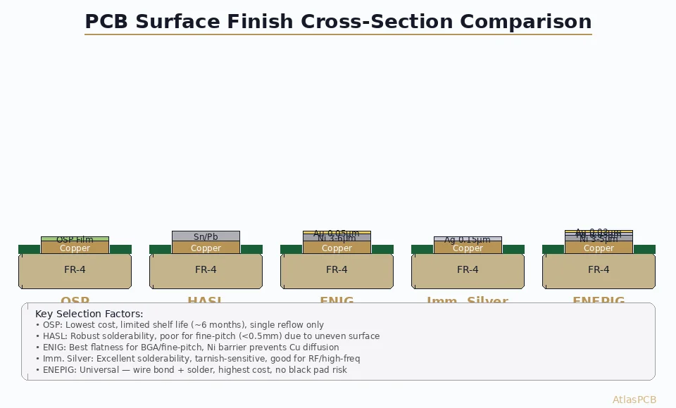
The Five Finishes at a Glance
HASL and Lead-Free HASL
Hot Air Solder Leveling coats pads with molten solder (traditionally Sn63/Pb37; now commonly SAC305 for lead-free), then blasts excess solder away with hot air knives. The result is a robust, highly solderable finish with excellent wetting characteristics.
Advantages: Lowest cost per square foot, proven long shelf life (>12 months), outstanding solderability, easy visual inspection of coating quality, reworkable.
Disadvantages: Inherently non-planar surface (solder meniscus creates domed pads), thermal shock during the leveling process can stress thin boards or PTH barrels, not suitable for fine-pitch components below 0.5 mm (20 mil) pitch due to uneven pad coplanarity, lead-free HASL runs at ~260 degrees C which limits substrate choices.
Governing standard: IPC-6012 (rigid board qualification) specifies minimum HASL thickness requirements; J-STD-003 covers solderability testing.
OSP (Organic Solderability Preservative)
OSP applies an ultra-thin (0.2-0.5 um) organic film — typically based on benzimidazole or substituted benzotriazole chemistry — onto clean copper. The film prevents oxidation while remaining transparent to the soldering process; flux in the solder paste dissolves the OSP during reflow.
Advantages: Lowest total process cost (even below HASL in high volume), perfectly flat/coplanar surface ideal for fine-pitch and BGA components, environmentally benign chemistry, no metallic contamination risk, simplest process line.
Disadvantages: Limited shelf life (typically 6 months under controlled storage, 3 months in humid environments), degrades with each thermal excursion (generally limited to 2-3 reflow cycles), not suitable for press-fit connectors or any contact/switch application, invisible finish makes inspection difficult, cannot withstand wire bonding.
Governing standard: IPC-6012, J-STD-003. OSP thickness and performance are also guided by supplier-specific data sheets (e.g., Shikoku Chemicals Glicoat series).
ENIG (Electroless Nickel Immersion Gold)
ENIG deposits a nickel barrier layer (typically 3-6 um per IPC-4552) topped with a thin immersion gold layer (0.05-0.15 um). The gold protects the nickel from oxidation and provides excellent solderability; during soldering, the gold dissolves into the solder and the joint forms between tin and the nickel barrier.
Advantages: Excellent planarity for fine-pitch and BGA, long shelf life (>12 months), good solderability, compatible with aluminum wire bonding, suitable for press-fit and membrane switch contacts, RoHS-compliant, well-established process with extensive industry data.
Disadvantages: Higher cost than HASL or OSP, susceptible to the black pad defect (hyper-corrosion of the nickel surface during gold deposition, causing brittle solder joints), not compatible with gold wire bonding (gold layer too thin), signal loss at high frequencies is higher than OSP due to nickel’s ferromagnetic properties (permeability and skin effect losses).
Governing standard: IPC-4552 Rev B — specifies nickel thickness 3.0-6.0 um, gold 0.05-0.15 um, and phosphorus content 7-10 wt% (mid-phos) in the nickel deposit.
For a detailed breakdown of the ENIG plating process, bath chemistry, and quality controls, visit our [ENIG surface finish process article]/blog/enig-surface-finish-process/).
Hard Gold (Electrolytic Nickel/Gold)
Hard gold — more precisely, electrolytic gold over electrolytic nickel — is deposited using an external electrical current, which means it requires bus traces (plating leads) routed to every pad that needs the finish. The gold layer is typically 0.75-1.25 um (30-50 uin) for edge connectors and up to 2.5 um for high-cycle applications. Cobalt or nickel hardening agents are co-deposited to achieve Knoop hardness of 130-200 HK.
Advantages: Exceptional wear resistance (withstands >1000 insertion cycles for edge connectors), lowest contact resistance among all finishes, excellent long-term reliability in contact and connector applications, very long shelf life (>24 months).
Disadvantages: Highest cost by a significant margin ($15-30+ per sqft premium over HASL), requires plating bus routing (adds design complexity, bus traces must be removed after plating), hardening agents (Co, Ni) in the gold can embrittle solder joints if not properly managed (gold embrittlement risk when thickness >0.5 um dissolves into solder), not used for general SMT soldering — reserved for connector fingers, test points, and switch contacts.
Governing standard: Hard gold for connectors follows MIL-G-45204 and ASTM B488.
ENEPIG (Electroless Nickel Electroless Palladium Immersion Gold)
ENEPIG adds a palladium interlayer (0.05-0.30 um per IPC-4556) between the nickel and gold. The palladium acts as a barrier that prevents the galvanic hyper-corrosion mechanism responsible for black pad in ENIG, while also providing a wire-bondable surface compatible with both gold and aluminum wire.
Advantages: Eliminates black pad risk, compatible with gold wire bonding, aluminum wire bonding, and soldering on a single finish, excellent planarity, long shelf life (>12 months), versatile “universal finish” suitable for mixed-technology boards.
Disadvantages: Highest cost among immersion finishes (palladium is expensive, and the additional plating step adds process time), relatively newer process with less long-term field data than ENIG, palladium thickness control is critical — too thin gives inadequate barrier, too thick can impair solderability due to Pd-Sn intermetallic formation.
Governing standard: IPC-4556 — specifies Ni 3.0-6.0 um, Pd 0.05-0.30 um, Au 0.03-0.10 um.
For a focused comparison of ENEPIG and ENIG, including wire bonding test data, refer to our [ENEPIG vs ENIG article]/blog/enepig-vs-enig/).
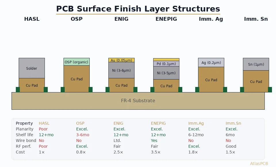
Comprehensive Comparison Table
| Parameter | HASL (Lead-Free) | OSP | ENIG | Hard Gold | ENEPIG |
|---|---|---|---|---|---|
| Typical Cost (relative) | 1.0x (baseline) | 0.8-1.0x | 1.5-2.0x | 3.0-5.0x | 2.0-3.0x |
| Cost per sqft (approx.) | $0.15-0.25 | $0.10-0.20 | $0.30-0.50 | $0.60-1.50+ | $0.45-0.75 |
| Shelf Life | >12 months | 6 months (controlled) | >12 months | >24 months | >12 months |
| Solderability | Excellent | Good (degrades w/ reflow) | Very Good | Fair (hard Au concerns) | Very Good |
| Max Reflow Cycles | 4-6 | 2-3 | 4-6 | N/A (not for reflow) | 4-6 |
| Surface Planarity | Poor (+/-20 um) | Excellent (+/-2 um) | Excellent (+/-5 um) | Good (+/-8 um) | Excellent (+/-5 um) |
| Fine-Pitch Capable (<0.5 mm) | No | Yes | Yes | No (bus trace limits) | Yes |
| Wire Bondable (Au wire) | No | No | No | Yes (soft gold variant) | Yes |
| Wire Bondable (Al wire) | No | No | Yes | Yes | Yes |
| Contact/Connector Use | No | No | Limited | Excellent | Good |
| Contact Resistance | N/A | N/A | 5-15 mohm | <2 mohm | 3-10 mohm |
| Insertion Cycle Rating | N/A | N/A | <50 cycles | >1000 cycles | <100 cycles |
| RoHS Compliant | Yes (LF version) | Yes | Yes | Yes | Yes |
| Black Pad Risk | None | None | Yes | None | None (Pd barrier) |
| IPC Standard | J-STD-003 | J-STD-003 | IPC-4552 | MIL-G-45204 | IPC-4556 |
| Rework Friendly | Excellent | Poor | Good | Good (connectors) | Good |
The Black Pad Problem — ENIG’s Achilles Heel
Black pad is the most discussed failure mode in surface finish technology. It occurs during the immersion gold deposition step of ENIG: the galvanic displacement reaction between gold ions and nickel can become locally aggressive, causing hyper-corrosion of the nickel surface. The corroded nickel forms a dark, phosphorus-enriched layer that prevents proper intermetallic bond formation during soldering.
Root Causes
Phosphorus content out of range: The electroless nickel deposit contains phosphorus from the reducing agent (sodium hypophosphite). IPC-4552 Rev B specifies 7-10 wt% phosphorus (mid-phos). Below 7%, the nickel is too active and corrodes aggressively during gold deposition. Above 10%, the deposit becomes overly amorphous and can develop micro-cracks.
Excessive gold deposition time or temperature: Longer immersion in the gold bath increases the galvanic attack on nickel. Gold thickness should be tightly controlled within the 0.05-0.15 um window.
Nickel bath age and loading: As the electroless nickel bath ages, stabilizer concentration, pH, and metal turnover rates drift, changing the deposit microstructure. Aged baths are more prone to producing nodular nickel that is susceptible to localized corrosion.
Pad geometry effects: Small pads, thermal pads with via connections, and pads with high aspect ratios can experience uneven nickel deposition, creating weak spots where hyper-corrosion initiates.
Mitigation Strategies
- Maintain electroless nickel phosphorus content within 8-9 wt% (tighter than the IPC spec range) for maximum resistance.
- Monitor gold bath chemistry aggressively — control gold metal concentration, pH (4.5-5.0), and temperature (+/-2 degrees C).
- Implement statistical process control (SPC) on nickel and gold thickness using XRF measurements on every production lot.
- Conduct cross-section analysis and solder joint pull/shear testing on a periodic basis.
- For high-reliability applications, consider migrating to ENEPIG, which structurally eliminates the galvanic corrosion pathway.
Phosphorus Content — Why It Matters
The phosphorus content in the electroless nickel layer fundamentally determines the deposit’s microstructure, corrosion resistance, solderability, and magnetic properties:
- Low-phos (2-5 wt%): Microcrystalline structure, higher hardness (~700 HV), magnetic, excellent wear resistance but poor corrosion resistance. Rarely used for PCB surface finish.
- Mid-phos (6-9 wt%): Semi-amorphous, good balance of corrosion resistance and solderability. The standard for ENIG and ENEPIG per IPC-4552/4556.
- High-phos (10-13 wt%): Fully amorphous, best corrosion resistance, non-magnetic. Used in applications requiring corrosion resistance (e.g., chemical environments) but can exhibit poorer solderability and is more prone to micro-cracking after thermal cycling.
For RF and high-speed digital applications, the magnetic properties of the nickel layer matter: mid-phos nickel is weakly ferromagnetic, contributing to insertion loss above 1 GHz. If signal integrity is paramount and ENIG is required, specifying high-phos nickel (>10 wt%) can reduce this loss, though the trade-off is the solderability concerns mentioned above. Alternatively, OSP eliminates the nickel layer entirely.
OSP Reflow Limitations — Understanding Thermal Budget
OSP’s organic film is consumed during each reflow cycle. The flux in solder paste dissolves the OSP to expose clean copper, allowing wetting. However, each thermal excursion (including any preheat or reflow on the opposite side of a double-sided board) partially degrades or volatilizes the remaining OSP on unsoldered pads.
Practical implications:
- Double-sided reflow: The first reflow pass (typically the top side) consumes much of the OSP on bottom-side pads. By the time the board is flipped for the second pass, remaining OSP may be insufficient for reliable wetting, especially on fine-pitch pads.
- Mixed assembly: If a board requires SMT reflow followed by wave or selective soldering, the through-hole pads may have endured 2-3 thermal cycles before they need to be soldered. OSP may not survive this.
- Rework: OSP-coated pads that have been through reflow but were not soldered (e.g., no-stuff pads, test points) will have degraded or eliminated OSP. Rework on these pads requires aggressive flux or micro-abrasion to remove the oxide layer.
Recommended practice: Limit OSP to designs with 2 or fewer reflow passes and minimal rework expectations. For complex assembly sequences, ENIG or ENEPIG provide more robust protection through multiple thermal cycles.
When to Use Each Finish
Choose HASL When:
- Cost is the primary driver and fine-pitch is not required
- Component pitch is at or above 0.65 mm (25 mil)
- Maximum solderability and rework capability are needed
- Board thickness is 1.0 mm or above (thin boards warp during HASL)
- Long shelf storage is expected in uncontrolled environments
Choose OSP When:
- Fine-pitch BGA and QFP components dominate the design
- Assembly will occur within 3-6 months of fabrication
- Assembly process is limited to 1-2 reflow passes
- Lowest possible cost is required at high volumes
- High-frequency signal integrity is critical (no nickel loss)
Choose ENIG When:
- Fine-pitch capability is needed with extended shelf life
- Boards will undergo multiple reflow and rework cycles
- Press-fit connectors or membrane switches are present
- Aluminum wire bonding is required
- A flat, inspectable surface is needed for automated optical inspection (AOI)
Choose Hard Gold When:
- Edge connectors with high insertion cycle requirements exist (PCIe, ISA, memory modules)
- Switch contacts, test pads, or probe points need wear resistance
- Contact resistance below 5 mohm is a design requirement
- Budget accommodates the premium cost
Choose ENEPIG When:
- Both gold wire bonding and SMT soldering are required on the same board
- Black pad risk must be eliminated for high-reliability applications (medical, aerospace, automotive)
- The board serves multiple functions (connectors + SMT + wire bond) requiring a universal finish
- Long shelf life, fine-pitch capability, and wire bondability are all simultaneously required
Mixed Finish Boards — Combining Finishes on One PCB
In some designs, no single finish satisfies all requirements. For example, a board might need hard gold on edge connector fingers, ENIG on SMT pads, and OSP on high-frequency RF sections. Mixed-finish (selective finish) processing is available from advanced fabricators, though it adds cost and complexity.
Common combinations:
- Hard gold fingers + ENIG body: The most common mixed finish. Hard gold is electroplated on connector fingers before the nickel/gold is stripped from SMT areas and ENIG is applied. This requires careful masking and process sequencing.
- Hard gold fingers + OSP body: Lower cost alternative when fine-pitch is needed without ENIG’s shelf life. Selective OSP is applied after hard gold plating.
- ENEPIG body + selective soft gold for wire bond pads: For advanced packaging, some fabricators can deposit thicker soft gold on wire bond pads while maintaining standard ENEPIG elsewhere.
Design considerations for mixed finish:
- Minimum spacing between finish zones is typically 20-30 mil (0.5-0.75 mm) for reliable masking.
- Communicate finish zones clearly on fabrication drawings with explicit callouts and dimensions.
- Verify that your fabricator has documented capability for the specific combination you need — not all shops support all combinations.
IPC Standards Reference
| Standard | Finish | Key Requirements |
|---|---|---|
| IPC-4552 Rev B | ENIG | Ni: 3.0-6.0 um, Au: 0.05-0.15 um, P: 7-10 wt% |
| IPC-4553 Rev A | Immersion Silver | Ag: 0.20-0.45 um (not covered in this comparison) |
| IPC-4554 | Immersion Tin | Sn: 0.8-1.2 um (not covered in this comparison) |
| IPC-4556 | ENEPIG | Ni: 3.0-6.0 um, Pd: 0.05-0.30 um, Au: 0.03-0.10 um |
| J-STD-003 | All | Solderability testing methods |
| MIL-G-45204 | Hard Gold | Type I/II/III classification by purity and hardness |
| ASTM B488 | Hard Gold | Electrodeposited gold coating requirements |
| IPC-SM-840 | Solder Mask | Qualification and performance (interacts with finish selection) |
Real Cost Analysis
Cost comparisons vary by region, volume, and board complexity, but the following ranges provide realistic guidance based on 2025-2026 market pricing for a standard 4-layer, 1.6 mm FR-4 board in panel quantities of 50+:
| Finish | Added Cost per sqft (panel) | Added Cost per Board (100x100 mm) | Notes |
|---|---|---|---|
| HASL (LF) | $0.15-0.25 | $0.02-0.04 | Baseline; most shops include in base price |
| OSP | $0.10-0.20 | $0.01-0.03 | Often cheaper than HASL at high volume |
| ENIG | $0.30-0.50 | $0.05-0.08 | Gold and nickel chemical costs dominate |
| Hard Gold | $0.60-1.50 | $0.10-0.25 | Selective finger plating; full-board hard gold is much higher |
| ENEPIG | $0.45-0.75 | $0.07-0.12 | Palladium cost adds ~30-50% premium over ENIG |
These figures cover the finish process cost only. Total board cost includes substrate, drilling, plating, imaging, and testing, of which the finish typically represents 5-15% for standard finishes and up to 25% for hard gold on large connector areas.
When evaluating cost, consider the total cost of ownership: a cheaper finish that causes field failures, requires rework, or limits shelf life may cost far more in the long run than a premium finish that delivers first-pass yield and long-term reliability.
Decision Framework — Putting It All Together
Start with your assembly requirements: What components are on the board? Fine-pitch BGA? Wire bonds? Edge connectors? This narrows the field immediately.
Evaluate your supply chain timing: If boards will sit in inventory for months, eliminate OSP. If you have just-in-time assembly, OSP becomes viable.
Consider your thermal budget: Count the total number of thermal excursions each pad will see (reflow passes, wave, selective, rework). If >2, avoid OSP.
Assess reliability requirements: Automotive, medical, and aerospace applications should default to ENIG or ENEPIG. Consumer electronics with short product lifecycles can use HASL or OSP.
Factor in signal integrity: For RF above 1 GHz, the nickel layer in ENIG/ENEPIG adds insertion loss. OSP or immersion silver (not covered here) may be preferred.
Optimize cost at the appropriate level: Do not save $0.03/board on surface finish if it creates a $3.00/board rework cost downstream.
For an overview of all available surface finishes including immersion silver and immersion tin, see our [PCB surface finish guide]/blog/pcb-surface-finish-guide/). If you are designing complex [multilayer PCBs]/blog/multilayer-fr4-pcb-manufacturer/) where finish selection interacts with stackup and via structure decisions, our engineering team at Atlas PCB can provide DFM review and finish recommendations tailored to your specific design.
Conclusion
There is no universally “best” surface finish — only the best finish for a given application’s requirements, assembly process, reliability targets, and budget. HASL remains the cost-effective workhorse for standard through-hole and coarse-pitch designs. OSP delivers unbeatable planarity and cost for high-volume, short-shelf-life, fine-pitch assembly. ENIG provides the versatile, reliable middle ground with excellent shelf life and process tolerance. Hard gold is indispensable for connector fingers and high-wear contacts. And ENEPIG emerges as the universal finish for mixed-technology boards demanding wire bondability and solderability without black pad risk.
By understanding the metallurgy, cost structure, process limitations, and IPC standards behind each finish, you can make confident, data-driven decisions that optimize both manufacturing yield and product reliability.
Further Reading
- [ENEPIG vs ENIG: Which PCB Surface Finish for Your Design?]/blog/enepig-vs-enig/)
- [Rogers PCB Fabrication: Material Sourcing, Lead Times & Quality Control]/blog/rogers-pcb-fabrication/)
- [ENEPIG vs ENIG Surface Finish: Complete Comparison for Wire Bonding, Solderability, and Long-Term Reliability]/blog/enepig-vs-enig-surface-finish-wire-bonding/)
- [PCB Surface Finish Comparison: OSP vs HASL vs Immersion Silver vs ENIG for Assembly Reliability]/blog/pcb-surface-finish-osp-hasl-enig-immersion-silver-comparison/)
- [mmWave PCB Material Selection: Rogers vs Megtron vs LCP for 5G and 6G Applications]/blog/mmwave-pcb-material-selection-rogers-megtron-lcp-5g-6g/)
- Rigid PCB Manufacturing
About AtlasPCB — We specialize in complex PCB manufacturing for HDI, RF, and high-reliability applications. Explore our RF and high-frequency PCB services, or get an full PCB manufacturing capabilities . Every order includes free engineering review. Get your quote.
Reviewed by AtlasPCB Engineering Team — IPC-certified manufacturing specialists with 15+ years of production experience in HDI, RF, and high-reliability PCB fabrication. Content based on factory floor data and real customer design reviews.
- surface finish
- ENIG
- HASL
- OSP
- hard gold
- ENEPIG
- PCB manufacturing