· AtlasPCB Engineering · Engineering · 10 min read
PCB Design for AI Optical Interconnect Modules: Material, Thermal, and Signal Integrity Requirements
Engineering guide to PCB substrate requirements for co-packaged optics and optical transceiver modules in AI data center infrastructure. Covers low-loss laminate selection, thermal management for VCSEL/driver ICs, and 56 GBaud signal integrity.

The Convergence of AI and Optical PCB Design
The explosive growth in AI cluster interconnect bandwidth is creating an entirely new class of PCB substrate requirements. When a single AI GPU requires 3.2 Tbps of optical I/O bandwidth—moving data between racks at 800G per port—the PCB substrate hosting the optical engine becomes a precision instrument rather than a commodity circuit board. Every material choice, every tolerance specification, every thermal pathway directly impacts whether photons couple efficiently between silicon and glass fiber.
This guide addresses the specific PCB engineering challenges introduced by optical interconnect modules for AI infrastructure: the transceiver modules (OSFP, QSFP-DD800) that populate rack switches, and the emerging co-packaged optics (CPO) that integrate photonics directly adjacent to the switch ASIC. Both demand PCB substrates that simultaneously achieve RF-grade signal integrity, aggressive thermal management, and mechanical precision that would be considered excessive in conventional PCB applications.
The investment landscape confirms this trend is accelerating, not plateauing. Dongshan Precision’s announcement this week of $1.2 billion in AI optical module capacity, combined with AT&S’s EUR 2 billion substrate expansion, signals that the supply chain is building infrastructure for optical interconnect demand that is at minimum 3-5x current volumes within three years.
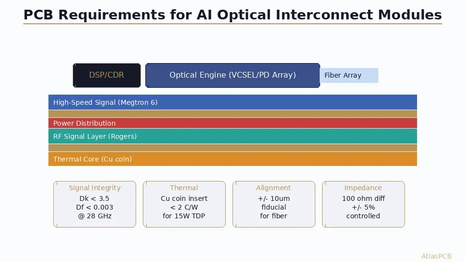
Signal Integrity at 56 GBaud: Material Selection Drives Everything
Optical module substrates carry PAM4 signals at 56 GBaud (112 Gbps per lane) from the host interface to the VCSEL/modulator driver IC. At these data rates, the PCB trace is the dominant loss mechanism between the connector and the IC die. A trace that performs adequately at 25 GBaud becomes a brick wall at 56 GBaud if the dielectric loss is not controlled.
The critical material parameter is dissipation factor (Df) at the Nyquist frequency. For 56 GBaud PAM4, the fundamental frequency component is 28 GHz with significant spectral content to 42 GHz. At 28 GHz, standard FR-4 (Df ~0.020) introduces approximately 2.5 dB/cm of loss in a microstrip configuration on 100-micron dielectric—meaning a 2cm trace loses 5 dB of signal amplitude before reaching the driver IC. The PAM4 eye closure budget simply cannot tolerate this.
Megtron 6 (Df 0.004 at 12.5 GHz, approximately 0.006 at 28 GHz) reduces this loss to approximately 0.8 dB/cm, enabling 3-4 cm trace lengths with equalization-recoverable signal quality. For the most demanding applications (200G/lane, 112 GBaud), next-generation materials like Panasonic Megtron 7 or Tachyon provide Df below 0.003 at 28 GHz—essential when trace lengths exceed 4 cm or loss budgets tighten due to reduced equalization capability in lower-power driver ICs.
The material selection has direct cost implications. Megtron 6 adds 3-4x material premium over FR-4, while ultra-low-loss materials can reach 5-8x. The hybrid stackup approach—placing premium material only on the two high-speed signal layers—optimizes cost without compromising performance because the electromagnetic field of a microstrip trace is concentrated within the first dielectric layer thickness below the conductor.
HIGH-SPEED PCB FABRICATION
Megtron 6, Low-Loss Hybrid Stackups — In Production
We fabricate 8-12 layer substrates with Megtron 6 signal layers, controlled impedance at 56 GBaud lane rates, and +/-5% tolerance. Upload your stackup for DFM review.
Get High-Speed Quote ›Thermal Management: Removing 15W from a 15mm Footprint
The thermal challenge in optical modules is extreme concentration. A single optical engine—comprising a VCSEL or EML array plus its driver IC—dissipates 10-15W in a package footprint of 10-15mm per side. The PCB substrate must transport this heat to a heatsink or chassis interface without allowing the junction temperature to exceed 85C (for VCSEL long-term reliability) or 105C (for driver ICs).
Conventional thermal via arrays provide a starting point but are insufficient alone for these heat flux densities. A standard thermal via array (0.3mm vias on 0.6mm pitch, non-conductive fill) achieves approximately 8-12 C/W through a 1.6mm board—acceptable for 3-5W components but inadequate for the 10-15W optical engine requirement. The temperature rise at 15W would be 120-180C above the board bottom temperature, pushing the VCSEL well past its reliability threshold.
The solution adopted by production optical module substrates is the embedded copper coin—a solid copper slug (typically 3-5mm thick, matching the optical engine footprint) press-fit or co-laminated into a cavity in the PCB substrate. The copper coin provides a near-zero thermal resistance path from the component attach surface to the board bottom, bypassing the laminate thermal resistance entirely. Combined with a ring of conductive-filled thermal vias surrounding the coin (to spread heat laterally into internal copper planes), effective thermal resistance drops to 2-3 C/W—keeping VCSEL junctions at 70-80C even at full power with a reasonable heatsink on the board bottom.
PCB fabrication of embedded copper coins requires precision cavity routing, controlled press-fit interference (typically 25-50 microns per side), and careful lamination pressure management to avoid resin starvation around the coin perimeter. Not all fabricators offer this capability—it requires specialized tooling and process validation that conventional PCB shops do not possess.
Impedance Control at Millimeter-Wave Frequencies
Impedance tolerance that is adequate for digital signaling becomes marginal at optical transceiver data rates. A +/-10% impedance tolerance on a 100-ohm differential pair creates 5% reflection at each impedance discontinuity. With multiple discontinuities along the signal path (via transitions, trace width changes, connector interfaces), these reflections compound to create intersymbol interference that degrades the PAM4 eye margin.
Production optical module substrates specify +/-5% impedance tolerance, with leading designs pushing toward +/-3% on critical differential pairs. Achieving this tolerance requires controlled dielectric thickness (requiring premium laminate with tighter thickness tolerance), narrower trace width tolerance (photolithography rather than conventional exposure for trace definition), and impedance test coupons measured at the operating frequency rather than the traditional 1 GHz TDR measurement.
The trace geometry itself evolves at these frequencies. Standard microstrip routing gives way to ground-backed coplanar waveguide (GCPW) with via fencing—providing better field containment, reduced radiation loss, and tighter impedance control. The via fence pitch must be less than lambda/4 at the highest frequency of interest (approximately 1.5mm at 50 GHz) to prevent lateral mode propagation. This via density requirement adds substantial drill count to the design but is non-negotiable for maintaining signal integrity at 56 GBaud and above.
PRECISION IMPEDANCE CONTROL
+/-5% Impedance at 28 GHz — Validated with VNA
TDR and VNA-verified impedance control for high-speed optical module substrates. GCPW routing with sub-1.5mm via fence pitch. Discuss your impedance budget with our SI engineer.
Discuss Requirements ›Mechanical Precision for Fiber Coupling
The most unusual PCB requirement in optical module fabrication is alignment precision. The substrate provides the mechanical reference frame for positioning the optical engine relative to the fiber array unit. While active alignment during module assembly handles the final micron-level positioning, the PCB must provide coarse alignment within the capture range of the alignment system—typically +/-50 microns for multimode systems and +/-10 microns for single-mode.
Achieving +/-10 micron fiducial placement accuracy on a PCB requires laser-defined alignment features rather than conventional photolithography. Standard PCB fabrication achieves +/-50-75 micron feature placement accuracy (referenced to board edge or drill pattern). Laser-ablated fiducials on copper or nickel surfaces can achieve +/-10-15 microns when referenced to precision tooling pins rather than board edges.
Additional mechanical requirements include flatness control (bow and twist less than 0.3% for proper die attach), controlled warpage during reflow (the substrate must remain flat enough that the optical engine maintains alignment after assembly thermal cycles), and surface roughness specification on the component attach area (Ra < 0.5 microns for reliable flip-chip bonding).
These requirements push the PCB substrate into a manufacturing regime that bridges conventional PCB fabrication and IC substrate processing. The fabricator needs capabilities in cavity routing, embedded metals, laser fiducial definition, and precision flatness measurement that go beyond standard multilayer PCB production.
Stackup Architecture for Optical Module Substrates
A representative 10-layer stackup for an 800G OSFP optical module substrate illustrates how these requirements combine:
| Layer | Function | Material | Thickness |
|---|---|---|---|
| L1 | High-speed signal (host-side) | Megtron 6 | 75 µm trace on 100 µm dielectric |
| L2 | Ground reference | Copper | 35 µm |
| L3 | Power (1.0V driver supply) | FR-4 core | 200 µm |
| L4 | Ground (isolation) | Copper | 35 µm |
| L5 | Low-speed control/I2C | FR-4 core | 200 µm |
| L6 | Ground (isolation) | Copper | 35 µm |
| L7 | Power (3.3V, host) | FR-4 core | 200 µm |
| L8 | Ground reference | Copper | 35 µm |
| L9 | High-speed signal (optics-side) | Megtron 6 | 75 µm trace on 100 µm dielectric |
| L10 | Ground/thermal | Copper | 70 µm |
The hybrid material approach confines expensive Megtron 6 to the L1 and L9 signal layers where RF performance matters, while using standard FR-4 cores for power distribution and low-speed control routing. This typically reduces material cost by 40-50% versus an all-Megtron construction while maintaining identical signal integrity on the critical high-speed lanes.
HDI microvias (0.1mm laser drill) connect the surface signal layers to internal ground references and enable BGA-pitch breakout under the driver IC. Through-board vias are reserved for power delivery and mechanical mounting, keeping them away from the high-speed signal transition areas where they would introduce impedance discontinuities.
HDI + LOW-LOSS MATERIALS
Complex Hybrid Stackups for Optical and AI Hardware
From 8-layer Megtron substrates to 24-layer HDI with embedded copper coins. We build the boards that connect photons to silicon.
The Market Opportunity: Why This Matters Now
The AI optical interconnect market is projected to grow from $4 billion in 2025 to over $15 billion by 2028, driven by the insatiable bandwidth requirements of GPU clusters and the physics-imposed limits of electrical interconnect beyond 2 meters. Every major hyperscaler is transitioning from 400G to 800G per port in 2026, with 1.6T ports already in development for 2027-2028 deployment.
Each 800G optical transceiver module requires a precision PCB substrate. A single AI cluster with 10,000 GPUs needs approximately 50,000-100,000 optical transceiver modules. The substrate demand this creates is enormous—and growing at 50%+ annually as AI training clusters scale from today’s 100,000-GPU installations toward the million-GPU facilities in planning for 2028.
For PCB fabricators positioned to serve this market, the opportunity combines high-value manufacturing (these substrates command $30-80 per piece at volume) with sticky customer relationships (qualification cycles of 6-12 months create high switching costs). The technical barrier to entry—requiring low-loss material processing, embedded metal capability, precision measurement, and HDI fabrication—limits competition to the top tier of PCB manufacturers globally.
ATLASPCB
Building AI Optical Hardware? Let's Talk Substrates.
We fabricate precision PCB substrates for optical transceiver modules. Megtron 6, embedded copper coins, HDI microvias, +/-5% impedance. From prototype to volume.
Start a Conversation ›Related Reading:
About AtlasPCB — We specialize in complex PCB manufacturing for HDI, RF, and high-reliability applications. Explore our impedance-controlled PCB manufacturing, or get an aluminum and metal-core PCB services . Every order includes free engineering review. Get your quote.
Reviewed by AtlasPCB Engineering Team — IPC-certified manufacturing specialists with 15+ years of production experience in HDI, RF, and high-reliability PCB fabrication. Content based on factory floor data and real customer design reviews.
- AI
- optical interconnect
- co-packaged optics
- PCB design
- signal integrity
- thermal management
- VCSEL
- data center