· AtlasPCB Engineering · Engineering · 8 min read
PCB Design Rule Check (DRC): Complete Manufacturability Checklist for Engineers
Definitive PCB DRC guide covering all critical design rule categories — clearance, width, annular ring, drill, plane, solder mask, and silkscreen rules — with specific values for standard, HDI, and advanced manufacturing capabilities, plus common violations and fixes.
Introduction: Why DRC Is Non-Negotiable
Every PCB design contains thousands of geometric relationships — trace-to-trace clearances, drill-to-copper distances, pad dimensions relative to holes, copper-to-board-edge margins. A complex 8-layer design might have 50,000+ individual checkable constraints.
Missing even one critical violation can result in:
- Opens: Traces etched too narrow break during fabrication
- Shorts: Inadequate clearance between conductors allows copper bridging
- Drill breakout: Holes positioned too close to copper features cause unintended connections
- Assembly failures: Solder mask dams too narrow allow solder bridging between pads
- Yield loss: Marginal dimensions pass at fabricator but fail at 20–40% rate during production
A thorough DRC with correct manufacturer constraints is the single most effective step you can take to prevent costly respins. Industry data shows that designs submitted with proper DRC reduce NPI (New Product Introduction) cycle time by 2–3 weeks on average.
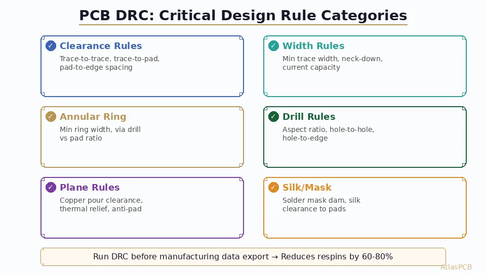
Category 1: Clearance Rules
Clearance rules ensure adequate spacing between all conductive features to prevent electrical shorts and meet dielectric withstand requirements.
Trace-to-Trace Clearance
| Feature Pair | Standard (≥4 mil) | Advanced (≥3 mil) | HDI (≥2.5 mil) |
|---|---|---|---|
| Signal to Signal | 100 μm (4 mil) | 75 μm (3 mil) | 63 μm (2.5 mil) |
| Signal to Power | 100 μm | 100 μm | 75 μm |
| Power to Power | 150 μm | 100 μm | 100 μm |
| Differential pair gap | Per impedance calc | Per impedance calc | Per impedance calc |
Voltage-Dependent Clearance (IPC-2221B)
For circuits exceeding 50V, clearance must increase based on working voltage:
| Peak Voltage | Internal Layer | External (Coated) | External (Bare) |
|---|---|---|---|
| 50V | 100 μm | 100 μm | 600 μm |
| 100V | 100 μm | 150 μm | 1.5 mm |
| 250V | 150 μm | 400 μm | 2.5 mm |
| 500V | 250 μm | 800 μm | 5.0 mm |
Pad-to-Pad Clearance
Adjacent component pads require sufficient spacing for:
- Solder mask dam between pads (minimum 75 μm mask web)
- Probe access for in-circuit testing (ICT)
- Rework iron access for component replacement
Minimum pad-to-pad: component pad edge to adjacent pad edge ≥ 150 μm (including mask expansion)
Copper-to-Board-Edge Clearance
| Edge Type | Minimum Clearance | Reason |
|---|---|---|
| Routed edge | 200 μm (8 mil) | Router bit tolerance + burr |
| V-score edge | 300 μm (12 mil) | Score blade registration |
| Tab-routed breakaway | 250 μm (10 mil) | Break line roughness |
| Connector edge (plated) | 500 μm (20 mil) | Housing insertion tolerance |
Category 2: Width Rules
Minimum Trace Width
| Copper Weight | Standard Process | Advanced Process | HDI/mSAP |
|---|---|---|---|
| 1/3 oz (12 μm) | 75 μm (3 mil) | 50 μm (2 mil) | 30 μm (1.2 mil) |
| 1/2 oz (18 μm) | 100 μm (4 mil) | 75 μm (3 mil) | 50 μm (2 mil) |
| 1 oz (35 μm) | 125 μm (5 mil) | 100 μm (4 mil) | 75 μm (3 mil) |
| 2 oz (70 μm) | 200 μm (8 mil) | 150 μm (6 mil) | — |
Neck-Down Rules
Trace width may reduce (“neck down”) when routing between tight-pitch BGA pads. Rules:
- Maximum neck-down length: 2× pad pitch (e.g., 1.6 mm for 0.8mm pitch BGA)
- Neck-down width ≥ 60% of nominal trace width
- Impedance discontinuity from neck-down: verify with field solver if length > λ/20 at signal bandwidth
Current-Carrying Capacity
DRC should enforce minimum widths based on current requirements (IPC-2152):
- External layer: 1A requires ~250 μm (10 mil) at 1 oz copper for 20°C rise
- Internal layer: 1A requires ~300 μm (12 mil) at 1 oz copper for 20°C rise
- Add 50% margin for production tolerances
Category 3: Annular Ring Rules
The annular ring is the copper pad remaining after a drill hole is made. Insufficient annular ring causes drill breakout (hole partially outside pad), creating unreliable connections.
Minimum Annular Ring Dimensions
| Via/Pad Type | Standard | Advanced | IPC Class 3 |
|---|---|---|---|
| Through-hole via | 125 μm (5 mil) | 100 μm (4 mil) | 150 μm (6 mil) |
| Component PTH | 175 μm (7 mil) | 150 μm (6 mil) | 200 μm (8 mil) |
| Microvia (laser) | 75 μm (3 mil) | 50 μm (2 mil) | 100 μm (4 mil) |
| BGA pad (NSMD) | 75 μm (3 mil) | 50 μm (2 mil) | 75 μm (3 mil) |
Calculation
Annular ring = (Pad diameter - Drill diameter) / 2
Example: 0.6mm pad with 0.3mm drill = (600-300)/2 = 150 μm ring ✓
Include registration tolerance: Actual annular ring = Designed ring - Registration error
- Standard registration: ±50 μm → Effective ring = 150 - 50 = 100 μm minimum achieved
Tangency and Breakout
IPC-6012 defines three conditions:
- Full annular ring: Hole completely within pad (ideal)
- Tangent: Hole edge touches pad edge (Class 1/2 acceptable)
- Breakout: Hole extends beyond pad (Class 3: max 90° of breakout)
Configure DRC to flag any via where minimum ring < required_ring + registration_tolerance.
Category 4: Drill Rules
Mechanical Drill Constraints
| Parameter | Standard | Advanced | Limitation |
|---|---|---|---|
| Min drill diameter | 0.20 mm | 0.15 mm | Bit deflection/breakage |
| Max aspect ratio | 10:1 | 12:1 | Plating throw |
| Hole-to-hole | 200 μm | 150 μm | Drill walk-off |
| Hole-to-board-edge | 300 μm | 200 μm | Routing bit proximity |
| Drill-to-copper (non-connected) | 200 μm | 150 μm | Registration tolerance |
Laser Drill (Microvia) Constraints
| Parameter | Standard | Advanced |
|---|---|---|
| Via diameter | 100–150 μm | 75–100 μm |
| Capture pad | 250 μm | 175 μm |
| Target pad | 250 μm | 175 μm |
| Aspect ratio | 1:1 max | 0.8:1 |
| Stacked vias | 2 high | 3 high (with fill+plate) |
Aspect Ratio Enforcement
Aspect ratio = Board thickness / Drill diameter
A 1.6mm board with 0.2mm drill = 8:1 aspect ratio. This is achievable but represents an advanced capability. DRC should flag:
- Standard process: aspect ratio > 8:1
- Via fills: aspect ratio > 6:1 (difficult to void-free fill)
- HDI builds: verify with fabricator for each specific stackup
Get AtlasPCB Design Rules
Download our complete DFM capability matrix with exact values for standard, advanced, and HDI processes — import directly into Altium or KiCad.
Category 5: Plane/Pour Rules
Copper Pour Clearance
Ground and power planes must maintain adequate clearance to signal vias/pads passing through:
| Feature | Standard | Advanced |
|---|---|---|
| Anti-pad (via clearance in plane) | 250 μm | 200 μm |
| Plane-to-trace clearance | 200 μm | 150 μm |
| Plane-to-board-edge | 500 μm | 300 μm |
| Plane-to-plane (different nets) | 250 μm | 200 μm |
Thermal Relief Design
Through-hole component pads connected to planes require thermal relief patterns for solderability:
- Spoke width: ≥ 200 μm (≥ trace minimum width)
- Spoke count: 4 spokes for standard components; 2 spokes for large thermal pads (to improve heat sinking)
- Relief gap: Same as anti-pad clearance (200–250 μm)
- Direct connect: BGA pads and thermal pads where maximum thermal conductivity is needed
Copper Balance
DRC should flag copper coverage imbalance between layers:
- Target: All layers within ±15% copper coverage of each other
- Critical threshold: >30% imbalance causes bow/twist during lamination
- Solution: Add copper thieving/hatching to low-coverage areas
Category 6: Solder Mask and Silkscreen Rules
Solder Mask Dam Width
The solder mask web between adjacent pad openings must be wide enough to prevent mask collapse during coating:
| Dam Width | Fabricator Capability | Notes |
|---|---|---|
| ≥ 100 μm (4 mil) | Standard | Reliable production |
| 75 μm (3 mil) | Advanced | Possible but may thin |
| 50 μm (2 mil) | LDI exposure only | Risk of bridging |
| < 50 μm | Mask between pads removed | Intentional solder mask defined |
Rule: If calculated mask dam < minimum, specify NSMD (Non-Solder-Mask-Defined) pads and remove mask between the pad cluster entirely.
Solder Mask Expansion
Standard mask opening = Pad size + expansion per side:
- Standard: +50 μm (2 mil) per side
- Fine-pitch (≤0.5mm): +25 μm (1 mil) per side
- BGA: Often 1:1 (mask opening = pad size) for NSMD
Silkscreen Rules
| Rule | Value | Reason |
|---|---|---|
| Min line width | 125 μm (5 mil) | Legibility after printing |
| Min text height | 800 μm (32 mil) | Readability |
| Silk-to-pad clearance | 100 μm (4 mil) | Prevent contamination |
| Silk-to-via clearance | 100 μm (4 mil) | Ink adhesion to mask |
| Silk over exposed copper | NOT ALLOWED | Solderability issue |
Setting Up DRC in Your EDA Tool
Altium Designer
- Navigate to Design → Rules → PCB Rules and Constraints
- Create rule categories matching the six categories above
- Set priorities: Manufacturing rules > electrical rules > signal integrity rules
- Enable Online DRC for real-time violation highlighting
- Import manufacturer constraint file if available (.RUL format)
KiCad 8+
- Open Board Setup → Design Rules → Constraints
- Define net classes with per-class clearance and width rules
- Use Custom Rules (.kicad_dru) for complex conditional checks:
(rule "BGA neck-down"
  (condition "A.NetClass == 'BGA_SIGNALS' && A.insideArea('BGA_FANOUT')")
(constraint track_width (min 0.075mm)))- Run DRC via Inspect → Design Rules Checker
Cadence Allegro
- Set up Physical and Spacing constraints in Constraint Manager
- Define constraint regions for area-specific rules (BGA region, high-voltage region)
- Configure DRC batch run with output to HTML report
- Enable real-time DRC with immediate visual markers
Common DRC Violations and Fixes
Top 10 Most Frequent Violations
- Clearance violation at BGA fanout: Reduce trace width with neck-down rule; or switch to HDI via-in-pad
- Annular ring too small on vias: Increase pad size or reduce drill diameter
- Trace too close to board edge: Move traces inward or increase board outline
- Solder mask dam too narrow: Switch to NSMD pad definition or increase pad pitch
- Unconnected copper fragments: Add copper pour with minimum area threshold (remove islands < 0.5 mm²)
- Acid trap (acute angle junction): Chamfer trace junctions to >90° angles
- Copper sliver: Thin copper fragments (<75 μm wide) that detach during etching — increase clearance or merge with adjacent copper
- Drill-to-copper violation: Increase anti-pad or move via away from trace
- Missing thermal relief on PTH pads: Add relief pattern in plane layers
- Silk over exposed pad: Auto-clip silkscreen at pad boundaries
When to Waive DRC Violations
Some violations are intentional and acceptable:
- Controlled-impedance traces narrower than standard minimum (verified by calculation)
- Edge connectors with copper extending to board edge
- RF structures with non-standard geometries (spiral inductors, coupled lines)
- Deliberate clearance reduction in specific zones (with fabricator approval)
Always document waivers in your design notes and confirm with your fabricator before release.
Further Reading
- PCB Design Rules: Trace Width and Spacing — Detailed trace geometry guidelines
- PCB Annular Ring and IPC Standards — Deep dive into ring requirements
- PCB Solder Mask Dam Design — Mask-specific DFM rules
- PCB Aspect Ratio and Via Design — Drill capability limits
Need DFM review for your next design? Submit your Gerber files to AtlasPCB for free manufacturability analysis with actionable feedback within 24 hours.
About AtlasPCB — We specialize in complex PCB manufacturing for HDI, RF, and high-reliability applications. Explore our free engineering DFM review . Every order includes free engineering review. Get your quote.
Reviewed by AtlasPCB Engineering Team — IPC-certified manufacturing specialists with 15+ years of production experience in HDI, RF, and high-reliability PCB fabrication. Content based on factory floor data and real customer design reviews.
- PCB DRC
- design rule check
- DFM
- manufacturability
- PCB design
- clearance rules
- annular ring
- Altium
- KiCad