· AtlasPCB Engineering · Engineering · 8 min read
IPC-A-600 PCB Acceptability Standard: Complete Visual Inspection Criteria and Classification Guide
Master IPC-A-600 acceptability criteria for bare PCB inspection. This comprehensive guide covers Class 1/2/3 requirements, common defect types, acceptance/rejection criteria for conductors, holes, surface finish, and solder mask — essential knowledge for quality engineers and procurement teams.
What Is IPC-A-600 and Why Does It Matter?
IPC-A-600, officially titled “Acceptability of Printed Boards,” is the global standard that defines what a “good” bare PCB looks like. Published by IPC (Association Connecting Electronics Industries), it provides visual criteria for inspecting printed circuit boards before they proceed to assembly.
Think of IPC-A-600 as the quality gate between PCB fabrication and PCBA assembly. Every board that arrives at an assembly house should be inspectable against IPC-A-600 criteria — and any board that fails these criteria represents either a reliability risk or a process control issue at the fabricator.
For procurement engineers, quality managers, and PCB designers alike, understanding IPC-A-600 is essential for:
- Writing purchase orders with clear quality requirements
- Receiving inspections that catch real problems without over-rejecting
- Supplier qualification based on objective, measurable criteria
- Design for manufacturability decisions that prevent rejection at inspection
This guide covers the complete IPC-A-600 framework with practical examples of how each criterion applies to modern PCB manufacturing.
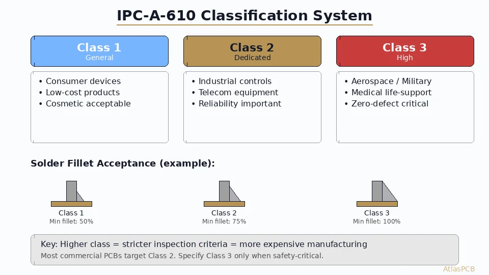
The Three Performance Classes
IPC-A-600 categorizes all electronic products into three classes, with progressively tighter acceptance criteria:
Class 1 — General Electronic Products
Consumer electronics, disposable devices, products where cosmetic imperfections are acceptable and occasional failure is tolerable.
Typical applications: LED lighting, simple IoT sensors, toys, basic consumer electronics
Key characteristics:
- Most permissive criteria
- Allows significant cosmetic variation
- Focus on basic functionality rather than long-term reliability
Class 2 — Dedicated Service Electronics
Products where continued performance and extended life are required but not critical to safety. This is the most commonly specified class.
Typical applications: Industrial controls, telecommunications equipment, commercial computing, automotive non-safety systems, point-of-sale terminals
Key characteristics:
- Moderate criteria balancing quality with manufacturing yield
- Most PCBs manufactured globally target Class 2
- Good balance between cost and reliability
Class 3 — High-Reliability Electronics
Products where continued performance is critical, downtime is unacceptable, or the operating environment is severe.
Typical applications: Life support systems, implantable medical devices, flight controls, military avionics, space systems, weapons systems
Key characteristics:
- Strictest criteria with minimum allowable defects
- Significantly higher manufacturing cost (15-40% premium)
- Requires full documentation and traceability
- Often combined with additional standards (MIL-PRF-31032, AS9100)
Conductor Inspection Criteria
Conductors (traces, pads, and planes) are the most critical feature on any PCB. IPC-A-600 defines specific acceptance criteria for their width, edge definition, and integrity.
Conductor Width Reduction
| Criterion | Class 1 | Class 2 | Class 3 |
|---|---|---|---|
| Maximum width reduction | 30% | 20% | 10% |
| Pinholes in conductor | Allowed if no bridging risk | ≤1 per inch, <50% width | None visible at 4× |
| Edge roughness | No limit if minimum width met | Smooth, minor nicks | Clean edges, no nicks |
Practical example: A 5 mil (0.127mm) trace designed at 5 mil:
- Class 2: Acceptable down to 4 mil at any point
- Class 3: Acceptable down to 4.5 mil at any point
Conductor Spacing
Reduced spacing between conductors is often more critical than width reduction because it directly affects insulation resistance and risk of electrical breakdown:
| Criterion | Class 1 | Class 2 | Class 3 |
|---|---|---|---|
| Minimum spacing reduction | 30% | 20% | 10% |
For a design with 5 mil spacing:
- Class 2: Minimum acceptable spacing is 4 mil
- Class 3: Minimum acceptable spacing is 4.5 mil
Lifted Conductors
Conductors must maintain adhesion to the substrate. IPC-A-600 addresses both lifted pads and lifted traces:
- Class 1/2: Minor lifting acceptable if conductor remains connected and no exposure of base material exceeds pad area
- Class 3: No lifted conductors acceptable; any visible separation constitutes rejection
Hole and Via Inspection
Drilled holes and vias are the three-dimensional backbone of multilayer PCBs. Their quality directly affects reliability under thermal cycling.
Annular Ring
The annular ring — the copper pad remaining around a drilled hole — is one of the most commonly inspected features:
| Criterion | Class 1 | Class 2 | Class 3 |
|---|---|---|---|
| Minimum annular ring | 0 (tangent allowed) | 1 mil (90° breakout max) | 2 mil (no breakout) |
| Breakout allowance | 180° | 90° | 0° |
What this means practically:
- Class 2: The drill can break out of the pad by up to 90°, meaning the hole touches the pad edge for up to one-quarter of its circumference
- Class 3: The hole must be completely contained within the pad with a minimum 2 mil annular ring at all points (360°)
Plating Thickness
Copper plating in through-holes directly affects reliability:
| Feature | Class 1 | Class 2 | Class 3 |
|---|---|---|---|
| Minimum barrel plating | 15 μm (0.6 mil) | 20 μm (0.8 mil) | 25 μm (1.0 mil) |
| Plating voids (barrel) | Allowed | <5% of barrel length | None |
| Corner crack (knee) | Not evaluated | Thin but continuous | ≥18 μm minimum |
Hole Wall Quality
Microsection analysis reveals the internal quality of plated through-holes:
- Positive etchback: Dielectric material recessed from copper (acceptable for all classes, preferred for Class 3)
- Negative etchback: Not permitted for Class 3
- Smear: Resin smear on inner layer connections must be removed (desmear process verification)
- Nail-heading: Copper foil deformation around holes — limited to 30% of interconnection width for Class 2
Need IPC Class 3 Boards with Full Microsection Reports?
AtlasPCB provides IPC-A-600 Class 3 manufacturing with coupon microsection analysis and complete quality documentation for medical, aerospace, and defense applications.
Request a Quote →Surface Finish Inspection
Surface finish quality affects solderability, shelf life, and long-term reliability. IPC-A-600 covers all common finishes:
ENIG (Electroless Nickel Immersion Gold)
| Criterion | Class 1 | Class 2 | Class 3 |
|---|---|---|---|
| Gold thickness | >0.03 μm | 0.05-0.15 μm | 0.05-0.15 μm |
| Nickel thickness | >2.5 μm | 3-6 μm | 3-6 μm |
| Black pad | Not evaluated | Reject if >5% of pads | Reject any occurrence |
| Coverage | 90% of solderable area | 95% of solderable area | 100% coverage |
HASL (Hot Air Solder Leveling)
| Criterion | Class 1 | Class 2 | Class 3 |
|---|---|---|---|
| Surface flatness | No spec | ±25 μm | ±15 μm |
| Solder bridging | Between pads: reject | Between pads: reject | Between pads: reject |
| Non-wetting | 20% area | 5% area | Not acceptable |
| Thickness | >1 μm | 1-25 μm | 1-25 μm, uniform |
OSP (Organic Solderability Preservative)
| Criterion | Class 1 | Class 2 | Class 3 |
|---|---|---|---|
| Coverage uniformity | Visual — no bare copper | Complete, uniform color | Complete, verified by thickness |
| Thickness | 0.2-0.5 μm | 0.2-0.5 μm | 0.2-0.5 μm |
| Discoloration | Allowed | Minor, if solderable | Not acceptable |
Solder Mask Inspection
Solder mask (LPI — Liquid Photoimageable) is the green (or other color) coating that protects copper and defines solder pads.
Registration
| Criterion | Class 1 | Class 2 | Class 3 |
|---|---|---|---|
| Mask on pad | 25% of pad area | 10% of pad area | Not acceptable |
| Mask in hole | Allowed | <25% of hole | Not acceptable |
| Clearance uniformity | No requirement | Visible but may vary | Uniform, centered |
Adhesion and Coverage
| Criterion | Class 1 | Class 2 | Class 3 |
|---|---|---|---|
| Bubbles/voids | Allowed | <1mm, not over conductors | Not acceptable |
| Peeling | >50% adhesion | <5% area | Not acceptable |
| Wrinkles/creases | Allowed | Minor, not over pads | Not acceptable |
| Thickness | >10 μm | 15-35 μm | 20-35 μm, uniform |
Laminate and Substrate Inspection
The base material of the PCB must meet specific quality standards:
Measling and Crazing
- Measling: White spots in the resin (separations between weave and resin)
- Crazing: White lines following the glass weave pattern
| Criterion | Class 1 | Class 2 | Class 3 |
|---|---|---|---|
| Measling | Acceptable | <10% of area between conductors | Not acceptable near conductors |
| Crazing | Acceptable | <10% of area | Not acceptable |
Delamination
Separation between any layer constitutes delamination:
- Class 1: Acceptable if <1% of total board area and not adjacent to holes or edges
- Class 2: Not acceptable if visible to the unaided eye or exceeds 0.5% of board area
- Class 3: Not acceptable — any delamination constitutes rejection
Bow and Twist
Board flatness (per IPC-TM-650 2.4.22):
| Criterion | All Classes |
|---|---|
| Maximum bow/twist (SMT) | 0.75% |
| Maximum bow/twist (through-hole only) | 1.5% |
Note: A 300mm board with 0.75% bow/twist may deflect up to 2.25mm — critical for fine-pitch BGA assembly.
HDI and Microvia-Specific Criteria (IPC-A-600K Addition)
The current revision (IPC-A-600K) added significant content for HDI structures:
Microvia Acceptance
| Feature | Class 2 | Class 3 |
|---|---|---|
| Via fill (resin plugged) | 50-100% fill | >80% fill |
| Dimple depth (filled vias) | <25 μm | <15 μm |
| Stacked via alignment | ±50 μm | ±25 μm |
| Microvia barrel crack | Not acceptable | Not acceptable |
| Target pad capture | 75% minimum | 90% minimum |
Sequential Lamination Defects
Multi-press HDI boards introduce unique defects:
- Layer-to-layer misregistration: Measured at coupon test targets, must meet IPC-6012 requirements for the class
- Resin recession at via-to-pad interface: Not acceptable for Class 3
- Sequential lamination delamination: Not acceptable for any class
Practical Inspection Implementation
Equipment Requirements
Effective IPC-A-600 inspection requires:
- Optical microscope: 10× to 40× magnification with ring illumination
- Stereo microscope: For 3D defect assessment
- Calibrated reticle/measurement tools: For width and spacing measurements
- Cross-section equipment: For destructive analysis (microsection)
- Reference standards: Current IPC-A-600K document with photographic illustrations
Sampling Plans
IPC-A-600 doesn’t mandate specific sampling plans — that’s covered by IPC-A-600’s companion documents and your quality system. Common approaches:
- Small lots (<100 boards): Inspect 100% for critical features, AQL sampling for cosmetic
- Production lots: Per IPC-2221 recommendation or customer-specific requirements
- Class 3: Often 100% inspection with additional coupon microsection per panel
Defect Documentation
When defects are found, proper documentation includes:
- Board serial number and lot identifier
- Feature location (reference designator, layer, coordinates)
- Defect classification (condition, not cause)
- Measurement data (if applicable)
- Photographic evidence at appropriate magnification
- Accept/reject disposition based on applicable class
Common Rejection Causes and Prevention
Based on industry data, the most frequent IPC-A-600 rejections are:
- Annular ring breakout (28% of rejections) — Prevention: Use ≥8 mil pads for ≥10 mil drill, add drill compensation in CAM
- Solder mask registration (22%) — Prevention: Specify ≥3 mil mask clearance, use LDI over screen printing
- Conductor width reduction (18%) — Prevention: Design with appropriate etch compensation, verify in DFM check
- Plating thickness variation (15%) — Prevention: Panel design with balanced copper distribution, proper rack design
- Surface finish defects (12%) — Prevention: Proper pre-cleaning, controlled immersion times, incoming material verification
Relationship to Other IPC Standards
IPC-A-600 doesn’t exist in isolation — it’s part of a standards ecosystem:
- [IPC-6012]/blog/news-ipc-6012-revision-es-via-fill-plating-2026/): Qualification and performance specification for rigid boards (defines what to build)
- IPC-A-600: Acceptability standard (defines how to inspect what was built)
- IPC-2221/2222: Design standards (defines how to design the board)
- IPC-A-610: Assembly acceptability (inspects the assembled board)
- IPC-TM-650: Test methods (how to measure specific properties)
The typical quality flow is: Design (IPC-2221) → Fabrication (IPC-6012) → Bare Board Inspection (IPC-A-600) → Assembly → Assembly Inspection (IPC-A-610)
Key Takeaways for Engineers and Procurement
- Always specify your class in purchase orders. “IPC Class 2” is the industry default, but don’t assume
- Understand the cost impact of Class 3: expect 15-40% premium due to tighter tolerances and higher scrap rates
- Focus inspection on critical features — annular rings, plating thickness, and registration are where most real reliability issues hide
- Use microsection data as your ground truth — visual inspection is a screen, but cross-section reveals the complete quality picture
- Build relationships with your fabricator — discuss rejection criteria before production, not after
Ready to get PCBs that consistently pass IPC-A-600 inspection? AtlasPCB maintains IPC-A-600 Class 3 manufacturing certification with in-house microsection analysis, automated optical inspection (AOI), and comprehensive quality documentation. Get your quote today →
About AtlasPCB — We specialize in complex PCB manufacturing for HDI, RF, and high-reliability applications. Explore our full PCB manufacturing capabilities . Every order includes free engineering review. Get your quote.
Reviewed by AtlasPCB Engineering Team — IPC-certified manufacturing specialists with 15+ years of production experience in HDI, RF, and high-reliability PCB fabrication. Content based on factory floor data and real customer design reviews.
- IPC-A-600
- PCB inspection
- quality control
- acceptability criteria
- visual inspection
- PCB defects
- Class 2
- Class 3
- bare board testing
- IPC standards