· AtlasPCB Engineering · Engineering · 6 min read
AI PCB Design Tools in 2026: From Copilot Assistants to Fully Autonomous Layout Engines
Explore the 2026 landscape of AI-powered PCB design tools — from KiCad AI plugins and Flux.ai cloud copilots to Quilter's end-to-end autonomous layout. Learn how AI is reshaping EDA workflows and what it means for PCB manufacturing.
The PCB design profession is undergoing its most significant transformation since the shift from tape-and-lightboard to CAD systems in the 1980s. AI-powered tools are not simply adding features to existing EDA platforms — they’re redefining what it means to “design” a PCB, compressing weeks of expert layout work into minutes and raising fundamental questions about the role of the PCB designer.
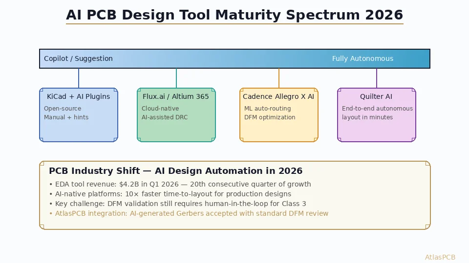
In Q1 2026, EDA tool revenue for PCB design reached $4.2 billion, marking the 20th consecutive quarter of growth. Much of this growth is fueled by AI features that make existing tools more productive and by entirely new AI-native platforms that approach PCB layout as a constraint-satisfaction problem solvable by machine intelligence.
This article maps the current landscape, evaluates what AI can and cannot do in 2026, and analyzes the implications for PCB manufacturers who receive AI-generated designs.
The AI Maturity Spectrum
AI PCB tools exist on a continuum from passive assistance to full autonomy:
Level 1: AI Suggestions (Copilot Mode)
Tools that offer recommendations but don’t execute design changes:
- Component placement suggestions based on datasheet reference designs
- DRC violation predictions before running full checks
- Bill of materials alternative recommendations
- Routing congestion heatmaps
Examples: KiCad AI plugins (community-developed), Flux.ai’s design assistant, Altium 365 component suggestions.
PCB designer role: Full control. AI provides information; human makes all decisions.
Level 2: AI-Assisted Execution
Tools that perform specific design tasks under human supervision:
- Auto-routing with ML-optimized cost functions (beyond traditional Lee/maze algorithms)
- Automatic DFM optimization (trace width adjustment, teardrop addition)
- Impedance-aware stackup suggestion based on signal requirements
- Thermal via array generation for power dissipation targets
Examples: Cadence Allegro X AI, Mentor/Siemens Xpedition AI, Altium Designer ML router.
PCB designer role: Defines constraints, reviews and accepts/rejects AI output, handles exceptions.
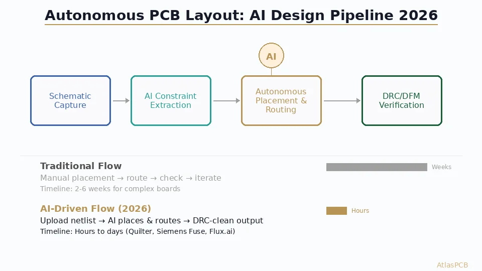
Level 3: Autonomous Layout (AI-Native)
Tools that generate complete layouts from constraints:
- Netlist-to-Gerber generation with minimal human input
- Simultaneous placement and routing optimization
- Constraint interpretation from schematic intent (not explicit rules)
- Automatic DRC resolution during generation (not post-check)
Examples: Quilter AI, DeepPCB (limited release).
PCB designer role: Defines design intent, validates output, handles DFM negotiation with manufacturer.
Key Players in 2026
Quilter AI: The Autonomous Layout Leader
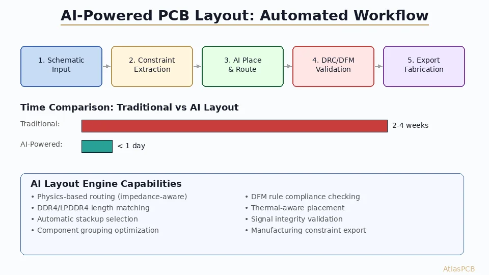
Quilter represents the most aggressive AI approach — treating PCB layout as a fully automatable process:
- Input: Schematic netlist + board outline + constraint set
- Output: Complete DRC-clean layout in 10-30 minutes (vs. days/weeks for manual)
- Capability: Proven on production designs up to 8 layers, ~500 components
- Claims: 10× faster time-to-layout than expert manual designers
Their “Project Speedrun” demonstrated autonomous layout of a functional computer — complete board designed, fabricated, and validated running under real workloads.
Limitations as of 2026:
- High-layer-count designs (12+) still challenging
- RF/analog sections require manual intervention
- Class 3 reliability validation remains human-dependent
- Cost-optimization for panelization not yet automated
Cadence Allegro X AI
The traditional EDA leader’s AI integration:
- ML-enhanced auto-routing that learns from design patterns
- Predictive DFM scoring before design completion
- Signal integrity-aware placement optimization
- Integration with Cadence’s simulation ecosystem (Sigrity, Clarity)
Strength: Deep integration with existing verification tools. Weakness: Still fundamentally an enhanced traditional tool, not AI-native.
Flux.ai: Cloud-Native AI-Assisted Design
Browser-based PCB design with AI assistance:
- Collaborative real-time design (similar to Figma for PCB)
- AI component selection and schematic suggestions
- Automated reference design adaptation
- Growing library of AI-verified design patterns
Strength: Accessibility and collaboration. Weakness: Limited to simpler designs, not production-competitive for complex boards.
Siemens Xpedition AI
Enterprise-focused AI for high-complexity designs:
- AI-driven BGA escape routing for 2000+ pin packages
- Thermal-aware placement optimization
- EMC prediction and mitigation suggestions
- Integration with manufacturing execution systems
What AI Handles Well vs. Where Humans Still Excel
AI Excels At:
- Routing optimization: Finding shortest/lowest-loss paths through congested regions
- Rule compliance: Maintaining thousands of design rules simultaneously
- Iterative placement: Testing millions of component arrangements for optimality
- Pattern matching: Applying proven layout techniques to similar circuits
- Speed: Minutes instead of days for standard designs
Humans Still Required For:
- Design intent interpretation: Understanding what the circuit is supposed to DO
- Manufacturing judgment: Knowing what’s theoretically possible vs. practically reliable
- Cost optimization: Panel utilization, layer count minimization, material selection trade-offs
- Reliability engineering: Thermal cycling, vibration, conformal coating considerations
- Novel circuits: First-of-its-kind designs without training data
Submit Your AI-Generated Design → | DFM Capabilities
Manufacturing Implications of AI-Generated Designs
What Manufacturers Are Seeing
PCB fabricators report increasing submissions of AI-generated Gerbers characterized by:
Positive patterns:
- Extremely consistent trace widths and spacing (no manual inconsistencies)
- Perfect DRC compliance (no rule violations)
- Optimized via placement for signal integrity
- Good impedance-controlled routing adherence
Concerning patterns:
- Aggressive minimum feature use (designs at exact minimum capability)
- Unusual copper distribution patterns (AI doesn’t naturally balance copper)
- Non-standard panelization assumptions
- Missing manufacturing notes that human designers would include
DFM Review Remains Critical
AI tools optimize for electrical performance within stated rules. They don’t inherently optimize for:
- Yield: Designs at minimum feature limits yield less than designs with margin
- Copper balance: Uneven copper distribution causes warpage and etching inconsistency
- Assembly: Component rotation for wave solder direction, panel breakaway clearance
- Test: Flying probe access, ICT pad placement for bed-of-nails fixtures
Adaptation Strategy for PCB Manufacturers
- Accept any source: Don’t discriminate between AI and human designs
- Standardize DFM checks: Apply identical review regardless of origin
- Provide design rules to AI tools: Publish actual manufacturing capabilities (not just minimums)
- Offer constraint files: Help AI tools target your specific process windows
The Economics of AI PCB Design
Cost Impact on Design Phase
| Design Type | Manual Design Cost | AI-Assisted | Fully Autonomous |
|---|---|---|---|
| Simple 2-layer | $2,000-5,000 | $1,500-3,000 | $200-500 |
| 4-6 layer standard | $5,000-15,000 | $4,000-10,000 | $500-2,000 |
| 8-layer HDI | $15,000-40,000 | $10,000-25,000 | $2,000-5,000* |
| 12+ layer complex | $40,000-100,000+ | $30,000-60,000 | Not yet feasible |
*With human validation pass
Impact on Time-to-Market
For startups and hardware companies:
- Prototype iteration: from weeks to days
- Design exploration: test multiple layout approaches in parallel
- Re-spins for manufacturing feedback: hours instead of re-design cycles
Impact on the Design Profession
The role is evolving from “layout technician” to “design architect”:
- Less time routing traces manually
- More time on constraint definition, validation, and manufacturing coordination
- Growing importance of manufacturing knowledge (what’s actually buildable)
- New skill: effective AI tool configuration and constraint programming
Looking Ahead: 2026-2028 Predictions
- Autonomous layout will handle 12+ layers by 2027 as training data and compute scale
- AI-to-manufacturer integration will enable direct constraint exchange (no more PDF datasheets)
- Simulation-in-the-loop AI will simultaneously route and verify SI/PI during layout
- Generative mechanical co-design will optimize PCB shape, connector placement, and enclosure simultaneously
- The “AI tax” — subscription pricing may make advanced tools inaccessible to small companies
Further Reading
- PCB DFM Checklist: Design for Manufacturability Guide
- Controlled Impedance PCB Stackup Design
- HDI PCB Stackup Design Advanced Guide
Conclusion
The AI PCB design landscape in 2026 is vibrant and rapidly evolving. For straightforward designs (≤ 8 layers, standard features), autonomous tools like Quilter deliver genuine 10× speedups that change project economics. For complex, high-reliability designs, AI serves as a powerful assistant that augments human expertise without replacing it.
For PCB manufacturers, the message is clear: be ready for AI-generated Gerbers, standardize your DFM review process, and publish your actual capabilities in machine-readable formats. The manufacturers who make it easiest for AI tools to target their process windows will capture the growing volume of AI-designed boards.
Submitting an AI-generated PCB design? AtlasPCB’s engineering team provides expert DFM review for AI-designed boards, catching manufacturing edge cases and optimizing for yield. Get started →
About AtlasPCB — We specialize in complex PCB manufacturing for HDI, RF, and high-reliability applications. Explore our full PCB manufacturing capabilities, or get an instant online quote . Every order includes free engineering review. Get your quote.
Reviewed by AtlasPCB Engineering Team — IPC-certified manufacturing specialists with 15+ years of production experience in HDI, RF, and high-reliability PCB fabrication. Content based on factory floor data and real customer design reviews.
- AI PCB design
- EDA tools
- autonomous layout
- Quilter AI
- design automation
- machine learning