· AtlasPCB Engineering · Engineering · 8 min read
EMC Shielding Techniques in PCB Layout: Ground Planes, Via Fencing, and Guard Traces
Comprehensive guide to PCB-level EMC shielding. Covers ground plane design, via stitching fences, guard traces, split plane management, and shield can integration for passing radiated emissions tests.
Why PCB-Level EMC Design Matters
Electromagnetic compatibility (EMC) is not an afterthought — it’s a fundamental design discipline that determines whether a product passes regulatory testing on the first attempt or requires costly redesigns. The PCB layout is where most EMC problems originate and where most solutions are implemented.
Every signal trace on a PCB is an antenna. Every return current path is a radiating loop. The difference between a clean design and a noisy one often comes down to understanding how electromagnetic fields propagate through and around the board structure — and strategically using copper, vias, and spacing to contain them.
Ground Plane Fundamentals
Why Ground Planes Are Your Primary Shield
A solid copper ground plane on a layer adjacent to your signal layer serves multiple EMC functions:
Return current confinement: High-frequency return currents flow in the ground plane directly beneath the signal trace (image current). Containing this current minimizes loop area and therefore radiation.
Field containment: Electric and magnetic fields from a microstrip or stripline are largely confined between the signal trace and reference plane. A continuous plane keeps these fields from radiating externally.
Shielding: From the opposite side of the plane, the continuous copper presents approximately 40–60 dB of isolation — signals on one side are effectively invisible from the other side.
Ground Plane Design Rules
Rule 1: No splits under high-speed signals
A split in the ground plane forces return current to detour around the slot, creating a large radiating loop. Even a 0.5 mm routing channel across a ground plane can increase emissions by 20 dB at harmonics.
If you must split a ground plane (e.g., for analog/digital isolation):
- Bridge the split with capacitors at every signal crossing point
- Route signals across the split at exactly one point (minimum slot interaction)
- Place the split far from board edges and I/O connectors
Rule 2: 20H rule for plane edges
The ground plane should extend at least 20× the dielectric thickness beyond the power plane edges on all sides. This prevents fringing fields at power plane edges from radiating. For a 0.1 mm dielectric: extend ground 2 mm beyond power plane edge.
Rule 3: Plane coverage ≥ 80%
Target ground plane copper coverage exceeding 80% after routing. Anti-pad clearances around through-hole vias and signal vias reduce coverage — plan via placement to maintain plane continuity in critical areas.
Rule 4: Stitch planes at the board edge
A ring of ground vias around the board perimeter (every 2–3 mm) connects all ground planes together and creates a faraday cage effect that reduces edge radiation.
Multi-Ground Plane Stackups
For EMC-critical designs, dedicate multiple layers to ground:
| Layer Count | Recommended Ground Layers | EMC Performance |
|---|---|---|
| 4 | L2 (full ground) | Good — single reference |
| 6 | L2, L5 (both ground) | Very good — dual shielding |
| 8 | L2, L4, L7 (triple ground) | Excellent — full containment |
| 10+ | Alternate signal/ground | Best — every signal is stripline |
The ideal EMC stackup places every signal layer between two ground planes (stripline configuration), eliminating external field exposure entirely.
Via Stitching and Via Fencing
How Via Fences Work
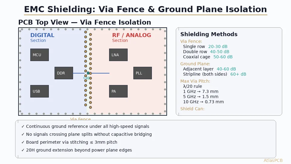
A via fence is a row (or double row) of ground vias connecting ground planes on multiple layers, creating a conductive wall that blocks electromagnetic energy propagation. The via fence acts as a waveguide wall — energy cannot pass through if the via spacing is significantly smaller than the wavelength.
Design Equations
Maximum via pitch for shielding effectiveness:
P_max = λ / 20 = c / (20 × f_max × √εr)
Where:
- P_max = maximum via pitch
- f_max = highest frequency to shield
- εr = dielectric constant of PCB material
- c = speed of light (3×10⁸ m/s)
| Frequency | εr = 4.2 (FR-4) | Max Via Pitch |
|---|---|---|
| 1 GHz | 146 mm wavelength | 7.3 mm |
| 3 GHz | 49 mm | 2.4 mm |
| 5 GHz | 29 mm | 1.5 mm |
| 10 GHz | 14.6 mm | 0.73 mm |
| 20 GHz | 7.3 mm | 0.37 mm |
Practical implication: For most digital designs with clock speeds up to 3 GHz (harmonics to ~15 GHz), a via pitch of 1.0–1.5 mm provides effective containment.
Via Fence Implementation
Single-row fence (standard isolation):
- Via drill: 0.25–0.30 mm
- Pitch: 1.0–2.0 mm (depending on frequency)
- Connected top and bottom to ground pours
- Provides ~20–30 dB isolation
Double-row fence (enhanced isolation):
- Two parallel rows of vias, staggered
- Row-to-row spacing: 0.5–1.0 mm
- Provides ~40–50 dB isolation
- Used around RF sections, PLL circuits
Coaxial via cage (maximum isolation):
- Full rectangular cage of vias surrounding a signal via or small area
- Six or more ground vias surrounding the target
- Provides ~50–60 dB isolation
- Used for single ultra-sensitive signals (reference clocks, LO distribution)
Where to Place Via Fences
- Between analog and digital sections — prevent digital switching noise from coupling into sensitive analog circuits
- Around RF front-ends — isolate LNA, mixer, PLL from digital baseband
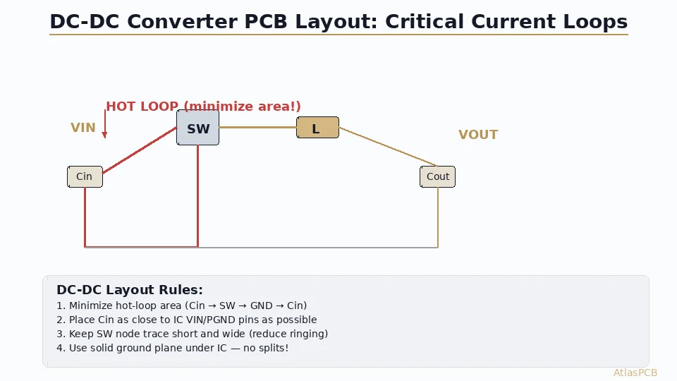
- Around switching regulators — contain magnetic field radiation from inductor and switching node
- At board edges — perimeter stitching prevents edge-fired radiation
- Around I/O connectors — contain common-mode currents that would otherwise radiate from cables
Complex EMC Layout Design?
AtlasPCB offers controlled-impedance boards with tight stackup tolerance for EMC-critical applications. Our DFM review catches common ground plane violations before production.
Get EMC-Optimized PCB Quote →Guard Traces and Coplanar Shielding
Guard Trace Design
A guard trace is a grounded conductor running parallel to a sensitive signal, providing lateral shielding:
- Width: Same as or wider than the signal trace
- Spacing: Place guard trace at 1–2× the trace-to-reference-plane distance
- Grounding: Via-stitch the guard trace every 3–5 mm (more frequent = better shielding)
- Length: Guard must extend at least 2 mm beyond the sensitive signal’s start and end
- Both sides: For maximum isolation, place guards on both sides of the victim signal
Guard traces are most effective for:
- Clock distribution lines adjacent to sensitive analog
- ADC reference routing near digital bus signals
- LVDS pairs running near single-ended high-speed signals
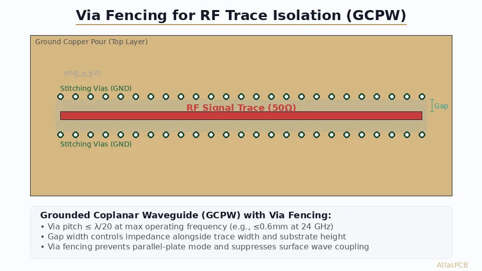
Coplanar Waveguide (CPWG) Shielding
For controlled-impedance signals that also need shielding, use a CPWG structure:
- Signal trace with ground coplanar on both sides (same layer)
- Ground plane reference on adjacent layer
- Via stitching connects coplanar ground to reference plane every 2–3 mm
- Achieves both impedance control and lateral EMI containment
CPWG is standard for:
- RF transmission lines above 1 GHz
- High-speed differential pairs in noise-sensitive environments
- Signals routed near board edges where return current paths may be compromised
Board-Level Shield (BLS) Can Integration
When Via Fencing Isn’t Enough
Metal shield cans (board-level shields) provide 50–90 dB isolation — far exceeding what via fences alone achieve. Use them when:
- Emissions testing shows specific frequency failures that PCB techniques can’t resolve
- You need guaranteed isolation between a transmitter and receiver on the same board
- Space doesn’t permit adequate separation between noisy and sensitive circuits
- The design has regulatory requirements (FCC Class B, CE) with tight margin
PCB Design for Shield Cans
Integrating shield cans requires PCB preparation:
- Shield can footprint: Create a continuous ground pad (0.5–1.0 mm wide) around the perimeter matching the can dimensions
- Via stitching under shield pad: Place vias every 1.5–2 mm along the shield footprint connecting to internal ground planes
- Component keepout: No components within 0.5 mm of shield can walls (thermal + mechanical clearance)
- Ventilation: Some shield cans have vent holes — ensure no sensitive traces route under vents
- Height clearance: Account for shield can height in mechanical stack (typically 1.5–3 mm)
- Removable option: Multi-piece shields allow rework access to shielded components
Shield Can Effectiveness
| Shield Type | Isolation (1 GHz) | Isolation (5 GHz) | Cost Impact |
|---|---|---|---|
| Single compartment can | 60–70 dB | 50–60 dB | +$0.30–1.00 |
| Multi-compartment frame | 50–60 dB | 40–50 dB | +$0.50–2.00 |
| Dual-wall (can + fence) | 70–80 dB | 60–70 dB | +$1.00–3.00 |
Split Plane Management
When Splits Are Necessary
Some designs require isolated power domains:
- Analog VCC separate from digital VCC
- Separate RF supply from baseband
- Mixed-signal ASICs with independent power pins
- Sensitive measurement circuits (medical, instrumentation)
EMC-Safe Split Plane Rules
Never split a ground plane — Use a common ground with via stitching instead. Separate power planes, not ground.
Capacitive bridging: Place decoupling capacitors (100 nF + 10 nF) at every point where a signal crosses a power plane split
Moat and bridge topology: Create a narrow bridge (2–3 mm wide) of common copper connecting the domains, with a single-point connection for low-frequency current
Signal routing discipline: Route ALL high-speed signals on layers with continuous reference planes. Never route signals on power plane layers that have splits.
Return current awareness: For any signal that must cross a power split, route it on a layer referenced to a continuous ground plane instead.
Testing and Verification
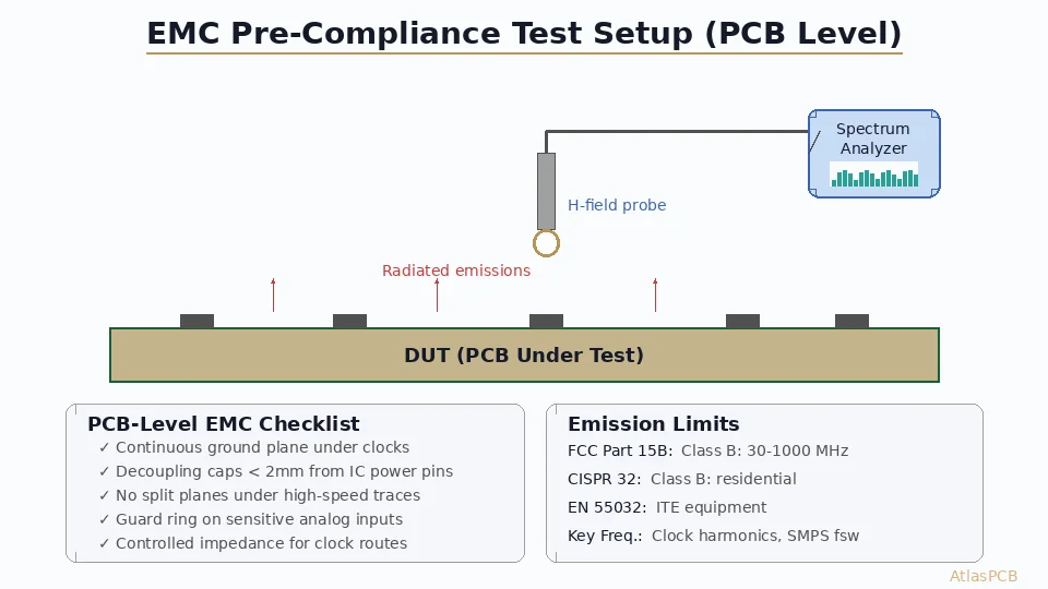
Pre-Compliance Measurements
Before formal EMC testing:
- Near-field probing: Use H-field (loop) and E-field (monopole) probes to identify radiation hotspots
- Spectrum analyzer scan: 30 MHz – 6 GHz sweep to identify problematic frequencies
- Current probe on cables: Measure common-mode current on all cables (often the primary radiation mechanism)
Common EMC Failures and PCB Root Causes
| Failure Mode | Frequency Range | Typical PCB Cause | Fix |
|---|---|---|---|
| Clock harmonic radiation | 300 MHz – 3 GHz | Signal crossing split plane | Fix return path or bridge split |
| Broadband noise | 30 – 300 MHz | Switching regulator loop | Tighten input cap placement, add shield |
| Specific frequency peak | Varies | Resonant cavity between planes | Add via stitching, reduce cavity size |
| Cable emission | All | No common-mode filtering at connector | Add CM choke, ground connector shell |
EMC Design Checklist Summary
✅ Continuous ground reference under all high-speed signals ✅ No signals cross plane splits without capacitive bridging ✅ Board perimeter via stitching at ≤3 mm pitch ✅ Via fence between analog/digital sections at ≤2 mm pitch ✅ Guard traces on sensitive signals with vias every 5 mm ✅ 20H ground plane extension beyond power plane edges ✅ Shield can footprints with stitched ground pads ✅ Decoupling capacitors within 1 mm of IC power pins ✅ Return current paths verified for every critical signal
Internal Links
- Review signal integrity and impedance control for related trace routing techniques
- Learn about PCB stackup design for optimal ground plane placement
- Explore RF PCB design with Rogers materials where EMC containment is critical
- Check thermal via arrays that also impact ground plane continuity
Designing a product that needs to pass FCC/CE emissions testing? Request a DFM review and our engineers will analyze your ground plane integrity, via stitching adequacy, and shield can integration before fabrication.
About AtlasPCB — We specialize in complex PCB manufacturing for HDI, RF, and high-reliability applications. Explore our precision rigid PCB manufacturing . Every order includes free engineering review. Get your quote.
Reviewed by AtlasPCB Engineering Team — IPC-certified manufacturing specialists with 15+ years of production experience in HDI, RF, and high-reliability PCB fabrication. Content based on factory floor data and real customer design reviews.
- EMC
- EMI shielding
- via fence
- ground plane
- guard trace
- PCB layout
- radiated emissions
- electromagnetic compatibility