· AtlasPCB Engineering · Engineering · 13 min read
PCB Ground Plane Stitching Vias: Placement Rules, EMI Reduction & High-Speed Design Guidelines
Learn PCB ground plane stitching via placement rules, spacing calculations, and EMI reduction strategies for high-speed and high-frequency circuit board designs.
What Are Ground Plane Stitching Vias?
Ground plane stitching vias are electrically connected vias that tie together ground planes (or power planes at the same potential) on different PCB layers. Unlike signal vias that carry data, stitching vias serve a purely structural electrical purpose: they maintain the ground reference system as a continuous, low-impedance conductor throughout the entire PCB volume.
Without stitching vias, ground planes on different layers are connected only at their edges (if at all) and behave as isolated resonant cavities at high frequencies. This creates problems:
- Return current discontinuity — when a signal changes layers, the return current must follow. Without a nearby stitching via, the return current must find a longer path, creating a loop antenna.
- Ground plane resonance — disconnected ground planes resonate at frequencies determined by their dimensions, creating voltage peaks that radiate EMI.
- Impedance discontinuity — the reference plane change at a signal via creates an impedance discontinuity that degrades [signal integrity]/blog/signal-integrity-pcb-design-guide/).
Stitching vias solve all three problems by providing short, low-impedance paths between ground planes at regular intervals.
The Physics Behind Stitching Via Effectiveness
Via Inductance and Impedance
A single via has a characteristic inductance determined by its geometry:
L_via ≈ (5.08 × h) × [ln(4h/d) + 1] nH
Where:
- h = via length (distance between connected planes) in inches
- d = via drill diameter in inches
For a typical stitching via (12 mil drill, 62 mil board thickness):
L_via ≈ (5.08 × 0.062) × [ln(4 × 0.062 / 0.012) + 1] ≈ 0.95 nH
At 1 GHz, this inductance represents approximately 6 Ω of impedance — significant compared to the milliohm resistance of the copper plane. Multiple parallel stitching vias reduce the effective inductance proportionally:
L_effective = L_via / N (for N parallel vias)
This is why a single stitching via is rarely sufficient at high frequencies — you need many vias in parallel to keep the inter-plane impedance low.
Wavelength and Spacing Rules
The fundamental spacing rule for stitching vias derives from electromagnetic wave propagation between parallel ground planes. When the spacing between vias exceeds a certain fraction of the wavelength, the gap between vias can act as a slot antenna, radiating energy.
The wavelength in the PCB dielectric:
λ = c / (f × √Dk)
Where:
- c = speed of light (3 × 10⁸ m/s)
- f = frequency of interest
- Dk = effective dielectric constant
The standard spacing rule:
Maximum via spacing ≤ λ/20
This ensures that the gap between adjacent stitching vias is too small relative to the wavelength to act as an efficient radiator.
| Frequency | λ in FR-4 (Dk≈4) | λ/20 Spacing |
|---|---|---|
| 1 GHz | 150 mm | 7.5 mm |
| 3 GHz | 50 mm | 2.5 mm |
| 5 GHz | 30 mm | 1.5 mm |
| 10 GHz | 15 mm | 0.75 mm |
| 20 GHz | 7.5 mm | 0.375 mm |
At 10 GHz and above, the λ/20 rule demands very tight via spacing — 0.75 mm or less — which can become a routing constraint. In these cases, some designers use λ/10 spacing (1.5 mm) as a practical compromise, accepting slightly degraded EMI performance.
Where to Place Stitching Vias
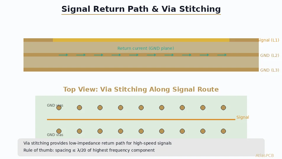
At Signal Layer Transitions
Every signal via needs adjacent stitching vias. When a signal changes routing layers, the return current must transition between the reference planes of the old and new layers. The stitching via provides the return current path.
Placement rules for signal transition stitching:
- Place at least one stitching via within 50 mil (1.27 mm) of every signal via
- For [differential pairs]/blog/differential-pair-routing-pcb/), place stitching vias on both sides of the pair’s via transition
- For high-speed signals above 5 Gbps, place two stitching vias flanking each signal via, one on each side
- The stitching via should connect the same planes that the signal’s reference changes between
This is not optional for high-speed design. A signal via without an adjacent stitching via creates a return current loop that radiates proportionally to frequency squared — a 10 GHz signal radiates 100× more from this loop than a 1 GHz signal.
For comprehensive via design guidance including stitching via integration, see our [via types guide]/blog/pcb-via-types-guide/).
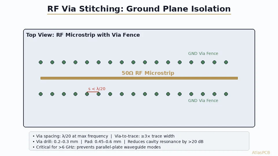
Along Board Edges
The edges of a PCB are significant EMI radiation sources. Electric fields between the ground plane edges fringe outward, creating “edge radiation” that increases with frequency.
Stitching vias along the board perimeter create a via fence that contains the inter-plane electromagnetic fields:
- Spacing: λ/20 at the highest frequency of concern
- Distance from edge: Place the via fence 50–100 mil (1.3–2.5 mm) from the board edge
- Continuity: The via fence should be continuous around the entire board perimeter, including around connectors and cutouts
- Ground plane extension: Extend the ground planes to the via fence (not beyond it, to avoid open-ended transmission line stubs)
For boards that must pass [EMC compliance testing]/blog/pcb-design-emi-compliance/), edge stitching is one of the most effective EMI mitigation techniques available.
Around Sensitive Signal Channels
High-speed routing channels carrying [controlled impedance signals]/blog/controlled-impedance-pcb/) benefit from stitching via fences on both sides:
- Channel isolation: Via fences between adjacent high-speed channels reduce [crosstalk]/blog/how-to-reduce-pcb-crosstalk/) by 10–20 dB compared to ground plane alone
- Via fence spacing: Use λ/20 spacing along the channel length
- Via fence width: A single row of vias provides meaningful isolation; double rows provide an additional 6–10 dB
This technique is essential for multi-channel high-speed interfaces (PCIe ×16, DDR bus, high-speed SerDes) where crosstalk between channels directly impacts bit error rate.
Near Connectors and I/O Interfaces
Connectors are the primary pathway for EMI to enter or exit a PCB. Dense stitching via placement around connector footprints:
- Provides low-impedance ground connection for connector shield pins
- Contains electromagnetic fields that leak through the connector transition
- Reduces ground bounce on I/O signals by lowering the ground path impedance
Placement guidance:
- Ring of stitching vias at λ/20 spacing around the entire connector footprint
- Connect to all ground planes, not just the surface ground
- Place stitching vias directly adjacent to connector ground pins (within 20 mil)
- For high-speed connectors, follow the connector vendor’s recommended via pattern
Around Ground Plane Slots and Splits
Any slot, cut, or split in a ground plane creates a discontinuity that forces return current to detour. Stitching vias cannot eliminate a slot’s effect, but they can minimize its radiation:
- Bridge vias: If the slot must exist (e.g., between different voltage domains), place stitching vias along both sides of the slot, connecting the ground plane segments on layers above and below the slotted plane
- Healing vias: Where a routing channel creates a de facto slot in a ground plane, place stitching vias between the traces to “heal” the gap
- Return path vias: At each point where a signal crosses a ground plane slot, place stitching vias to provide a return current path around the slot
For deeper coverage of ground plane design strategies, see our guide on [ground plane and copper pour design]/blog/pcb-copper-pour-ground-plane-design/).
Stitching Via Design Parameters
Via Geometry
Standard stitching vias use the same geometry as signal vias:
- Drill diameter: 8–12 mil (0.2–0.3 mm) for standard through-hole vias
- Pad diameter: Drill + 8–10 mil minimum annular ring (per IPC-6012 Class 2/3)
- Antipad clearance: 5–8 mil clearance to non-connected planes
For HDI designs, microvias (4–6 mil drill) can serve as stitching vias between adjacent layers, allowing tighter spacing without consuming as much routing area.
Via Pattern Options
Several stitching via patterns are commonly used:
Linear fence: A single row of vias at regular spacing. Simple to implement, effective for edge stitching and channel isolation.
Staggered double row: Two rows of vias with offset positioning. Provides better isolation than a single row because there is no direct line-of-sight gap between the rows.
Grid pattern: A rectangular array of vias filling an area. Used beneath shielding cans, around sensitive analog circuits, and in ground fill areas.
Via-in-pad ground array: Stitching vias placed in ground pads of BGA and other array packages. These serve double duty — providing ground connection for the component and stitching between ground planes. Ensure these are [filled and plated over]/blog/pcb-via-in-pad-plated-over-design/) per the assembly requirements.
Electrical Performance Modeling
For critical designs, model the stitching via structure using a 3D electromagnetic field solver. Key parameters to extract:
- Inter-plane impedance vs. frequency: Should remain below 1 Ω up to the highest frequency of concern
- Resonant frequencies: Identify and verify that no resonances occur within the signal bandwidth
- Isolation between channels: Verify that via fences provide the required isolation
Compare the modeled performance against the via spacing rule to determine if the λ/20 guideline is adequate or if tighter spacing is needed.
Impact on EMI Performance
Cavity Resonance Suppression
Parallel ground planes form a cavity that resonates at frequencies determined by the plane dimensions and dielectric properties:
f_mn = (c / (2 × √Dk)) × √((m/a)² + (n/b)²)
Where:
- m, n = mode numbers (integers)
- a, b = plane dimensions
For a 100 × 100 mm board with Dk = 4.0:
- f₁₀ = 750 MHz
- f₁₁ = 1.06 GHz
- f₂₀ = 1.50 GHz
At these resonant frequencies, voltage peaks appear across the plane pair, causing EMI spikes. Stitching vias suppress these resonances by breaking the cavity into smaller sub-cavities with higher resonant frequencies.
If stitching vias divide the 100 × 100 mm cavity into a 5 × 5 grid of 20 × 20 mm sub-cavities, the lowest resonant frequency shifts to:
f₁₀ = (3 × 10⁸) / (2 × √4 × 0.020) = 3.75 GHz
This pushes the resonances above the frequency range of most digital signals, effectively eliminating the cavity resonance problem.
Edge Radiation Control
Board edges radiate because the inter-plane electric field terminates abruptly, creating a fringing field that couples to the surrounding environment. The radiated power from a board edge is proportional to:
- The square of the voltage across the plane pair at the edge
- The square of the frequency
- The edge length
Stitching vias along the edge serve two purposes:
- Equipotential forcing — they drive the voltage across the plane pair toward zero at the edge, reducing the driving force for radiation
- Current path shortening — they provide short return current paths that reduce the effective loop area of edge currents
In practice, a continuous stitching via fence at λ/20 spacing along the board edge reduces edge radiation by 10–20 dB across the frequency range of interest.
For more [EMC/EMI design techniques]/blog/emc-emi-pcb-design/), our comprehensive guide covers additional strategies beyond stitching vias.
Return Current Management
When a signal trace transitions between layers through a via, the return current on the reference plane must also transition. The physics:
- Signal on Layer 3 has return current flowing on the adjacent ground plane (Layer 2)
- Signal transitions through a via to Layer 6, where the return current should flow on the adjacent ground plane (Layer 7)
- The return current must transition from Layer 2 to Layer 7
Without a stitching via, this current must flow across the entire board to find a connection between the planes — creating a large loop that radiates effectively as an antenna.
With a stitching via adjacent to the signal via, the return current transitions directly between planes with a loop area of only a few square millimeters. The EMI reduction is proportional to the reduction in loop area — often 20–30 dB.
Integration with Stackup Design
Stitching Vias and Layer Allocation
During [stackup design]/blog/pcb-stackup-design-guide/), plan for stitching vias from the beginning:
- Ground plane pairing: Ensure every signal layer has an adjacent ground plane that stitching vias can connect to the board’s primary ground system
- Power plane islands: Power planes with different voltages create natural splits. Plan stitching vias to connect ground pours on power plane layers back to the ground planes.
- Via span optimization: For multilayer boards with 12+ layers, consider using blind or buried stitching vias that connect only the relevant plane pairs, preserving routing space on unrelated layers
Routing Space Impact
Every stitching via consumes routing space on all layers it passes through. For a 12-mil drill with 22-mil pad and 8-mil clearance, each via blocks a 38-mil diameter circle on every layer.
Strategies to minimize routing impact:
- Use smaller drill sizes where possible (8 mil drill reduces the blocked area by approximately 35% compared to 12 mil)
- Place stitching vias in ground pour areas where routing is not needed
- Use microvias for adjacent-layer stitching in HDI designs — these only affect two layers instead of all layers
- Align stitching vias on a regular grid that the router can anticipate and route around
Thermal Via Dual-Purpose Design
In many designs, [thermal vias]/blog/pcb-thermal-via-design/) beneath power components also function as stitching vias, connecting ground planes while conducting heat. This dual-purpose approach:
- Maximizes thermal conductivity from the component pad to internal ground planes
- Provides excellent ground stitching in areas with high current density
- Reduces the total via count compared to separate thermal and stitching via arrays
Design thermal stitching vias with the same spacing rules as standard stitching vias, plus additional thermal analysis to verify adequate heat spreading.
Practical Design Example: 8-Layer High-Speed Board
Consider an 8-layer multilayer PCB stackup designed for 10 Gbps SerDes signals:
Stackup:
- L1: Signal (top, microstrip)
- L2: Ground
- L3: Signal (stripline)
- L4: Power
- L5: Ground
- L6: Signal (stripline)
- L7: Ground
- L8: Signal (bottom, microstrip)
Stitching via plan:
- Signal transitions L1↔L3: Stitch L2 to L5 ground planes adjacent to each signal via
- Signal transitions L3↔L6: Stitch L2/L5 ground planes (and bridge across L4 power plane)
- Edge fence: Continuous stitching connecting L2, L5, L7 at 1.5 mm spacing around the perimeter
- SerDes channel fences: Stitching via rows on both sides of each differential pair channel, connecting L2 and L5 at 1.5 mm spacing
- Connector area: Dense stitching grid at 1.0 mm spacing around high-speed connector footprints
Total stitching via estimate for a 100 × 150 mm board:
- Edge fence: approximately 340 vias
- Signal transitions: approximately 200 vias (varies with design)
- Channel fences: approximately 500 vias
- Connector areas: approximately 150 vias
- Total: approximately 1,200 stitching vias
This is typical for a moderately complex high-speed design. The manufacturing cost impact is minimal — primarily the additional drill hits.
Common Mistakes and How to Avoid Them
Mistake 1: Forgetting Stitching at Layer Transitions
Problem: Signal vias without adjacent ground stitching vias, creating return current loops.
Solution: Make it a design rule check (DRC) rule — every signal via must have at least one stitching via within a defined radius (50 mil for general high-speed, 30 mil for 10+ Gbps).
Mistake 2: Inconsistent Edge Stitching
Problem: Stitching via fence has gaps at connector cutouts, mounting holes, or board notches.
Solution: Maintain stitching continuity around all board edge features. Route the via fence around cutouts rather than stopping at them.
Mistake 3: Stitching Only Between Adjacent Ground Planes
Problem: In a stackup with ground planes on L2, L5, and L7, stitching vias only connect L2↔L5 and L5↔L7 but not L2↔L7 directly.
Solution: Through-hole stitching vias naturally connect all ground planes. If using blind vias, ensure there is at least one continuous path from every ground plane to every other ground plane through the stitching via network.
Mistake 4: Stitching Vias Creating Antipad Gaps in Signal Planes
Problem: Through-hole stitching vias create clearance holes (antipads) on signal layers, fragmenting routing channels.
Solution: Place stitching vias outside routing channels, or use blind/buried vias that only span the required ground plane pairs. In [16-layer stackups]/blog/16-layer-pcb-stackup-design/), this requires careful via planning during the stackup definition phase.
Conclusion
Ground plane stitching vias are the connective tissue that turns isolated copper layers into a functional ground system. Their placement follows clear engineering rules — λ/20 spacing for EMI control, adjacent placement at every signal layer transition, and continuous fencing along board edges.
The investment in stitching vias is small: standard through-hole vias at minimal manufacturing cost. The return is significant: 10–20 dB EMI reduction, consistent return current paths, and elimination of ground plane resonance that can create unpredictable behavior at high frequencies.
For any design operating above 1 GHz — or any design that must pass EMC compliance — stitching vias are not optional. They are a fundamental element of competent PCB design.
Ready to optimize your ground system design?
Upload your Gerbers for a free engineering review — our signal integrity team will evaluate your ground plane strategy, stitching via placement, and EMI risk areas. Get a quote today →
Further Reading
- [BGA Pad Design and Via-in-Pad: How to Prevent Solder Voiding in High Pin-Count BGA Assemblies]/blog/bga-pad-design-via-in-pad-solder-voiding-prevention/)
- [Via-in-Pad Design: Filled, Capped, and Plated Over — Complete Guide]/blog/via-in-pad-design/)
- [PCB Thermal Management: Heat Dissipation Techniques for Reliable Electronics]/blog/pcb-thermal-management/)
- [Press-Fit Via Design for PCB Connectors: Hole Sizing, Plating & IPC Compliance]/blog/pcb-press-fit-via-design/)
- [PCB Copper Plating Process: Electroless vs Electrolytic Copper for HDI Vias and High-Density Interconnects]/blog/pcb-copper-plating-electroless-vs-electrolytic-hdi-vias/)
- HDI PCB Manufacturing
About AtlasPCB — We specialize in complex PCB manufacturing for HDI, RF, and high-reliability applications. Explore our impedance-controlled PCB manufacturing . Every order includes free engineering review. Get your quote.
Reviewed by AtlasPCB Engineering Team — IPC-certified manufacturing specialists with 15+ years of production experience in HDI, RF, and high-reliability PCB fabrication. Content based on factory floor data and real customer design reviews.
- stitching-vias
- ground-plane
- emi
- shielding
- high-speed