· AtlasPCB Engineering · Engineering · 12 min read
PCB Design for EMI Compliance: A Practical Guide to Passing Radiated and Conducted Emissions Tests
Learn how to design PCBs that pass EMI compliance testing. Covers grounding strategies, shielding techniques, filtering, component placement, and layout best practices for FCC, CE, and CISPR standards.
Electromagnetic interference (EMI) compliance is not optional — it is a regulatory requirement in every major market. Products sold in the United States must meet FCC Part 15 limits, European markets require CE marking under the EMC Directive, and virtually every other region enforces equivalent standards based on CISPR 32 (for multimedia equipment) or CISPR 11 (for industrial, scientific, and medical devices).
The frustrating reality is that most EMI failures are caused by PCB design decisions, not by component defects or firmware bugs. A board that was never designed with EMI in mind will almost certainly fail compliance testing — and fixing EMI problems after fabrication typically costs 2–10× more than designing them out from the beginning.
This guide covers the PCB design principles and techniques that consistently lead to first-pass EMI compliance.
Understanding EMI: Sources, Paths, and Antennas
Every EMI problem has three elements:
- Source: A circuit that generates high-frequency energy (switching regulators, digital clocks, high-speed buses, PWM signals)
- Coupling path: The mechanism that transfers energy from source to antenna (conducted on traces/cables, radiated through space, or coupled through parasitic capacitance/inductance)
- Antenna: A structure that efficiently radiates energy into free space (cables, PCB traces, connector pins, IC leads, ground plane edges)
Effective EMI design addresses all three: reduce the source energy where possible, interrupt the coupling paths, and minimize antenna efficiency.
The Loop Area Principle
The single most important concept in PCB EMI design is current loop area. Every signal current flows in a loop — out through the signal trace and back through the return path (typically the ground plane). The electromagnetic field radiated by this loop is proportional to:
E ∝ f² × I × A
Where f is frequency, I is current, and A is the loop area. This means:
- Doubling the frequency increases radiation by 4× (12 dB)
- Doubling the loop area increases radiation by 2× (6 dB)
- A 10× increase in loop area increases radiation by 20 dB
This is why return path management is the foundation of EMI-compliant PCB design.
Grounding Strategies for EMI Control
Continuous Ground Planes
A continuous, unbroken ground plane is the single most effective EMI mitigation technique available to the PCB designer. It works by:
- Minimizing loop area: Return current flows directly beneath the signal trace on the ground plane (the path of least inductance), creating the smallest possible loop.
- Providing shielding: The ground plane acts as a Faraday shield between layers.
- Supporting controlled impedance: A uniform ground plane enables predictable impedance, reducing reflections that generate harmonics.
Critical rules for ground planes:
- No slots or splits under high-speed signal traces. A slot in the ground plane forces return current to detour around it, dramatically increasing the loop area. Even a 20-mil slot can increase emissions by 10–20 dB at GHz frequencies.
- Minimize via antipads in high-speed routing areas. Dense via fields can create a “Swiss cheese” effect in the ground plane, disrupting return currents.
- Stitch ground planes together between layers with vias at intervals of λ/20 or less at the highest frequency of concern.
For comprehensive grounding techniques, see our [PCB grounding techniques guide]/blog/pcb-grounding-techniques/).
Ground Plane Partitioning
In mixed-signal designs, the ground strategy requires careful thought:
| Approach | When to Use | EMI Impact |
|---|---|---|
| Single solid ground | Most digital designs, simple mixed-signal | Best — lowest impedance, no return path disruption |
| Star ground (single point) | Low-frequency analog (<1 MHz) with separate analog/digital sections | Good for conducted emissions, poor for radiated above 10 MHz |
| Split ground with bridge | Sensitive analog + noisy digital, bridge at ADC/DAC | Acceptable — bridge width is critical, keep it wide |
| Separate ground planes | Never recommended | Poor — creates large antenna loop between connectors |
Modern best practice: Use a single solid ground plane and manage noise through component placement and routing discipline rather than plane splits. This is recommended by virtually all major IC manufacturers for designs operating above 10 MHz.
Decoupling and Power Distribution
Inadequate decoupling is the second most common cause of EMI failures (after return path problems). High-speed ICs draw transient current during switching, and if the power distribution network cannot supply this current locally, the resulting voltage fluctuations radiate.
Decoupling Capacitor Placement Rules
Place decoupling capacitors within 2 mm (80 mils) of the IC power pins. At 1 GHz, the self-inductance of a 5mm trace section is roughly 3.5 nH — enough to negate the benefit of the capacitor.
Connect capacitors to the ground plane with short, wide traces or direct via connections. The via inductance (typically 0.5–1 nH per via) is often the dominant parasitic. Use two vias per pad where possible.
Use appropriate capacitor values for the frequency range:
| Frequency Range | Capacitor Value | Package Size | Notes |
|---|---|---|---|
| DC – 10 MHz | 10 µF | 0805 or larger | Bulk bypass, tantalum or ceramic |
| 10 – 100 MHz | 100 nF | 0402 | Standard decoupling |
| 100 MHz – 1 GHz | 10 nF | 0201 | High-frequency bypass |
| 1 – 5 GHz | 1 nF | 0201 | Very high frequency |
| >5 GHz | 100 pF | 0201 | Only effective with minimal parasitics |
Use multiple capacitor values in parallel to cover a broad frequency range. The parallel combination provides low impedance across decades of frequency.
Place a bulk capacitor (10–100 µF) near where power enters the PCB to handle low-frequency transients and provide energy storage.
Power Plane Design
- Keep power planes as close to ground planes as possible — the thin dielectric forms a distributed capacitor that provides high-frequency bypass.
- Avoid routing high-speed signals over power plane splits. The return current cannot cross the split, creating the same loop area problem as a ground plane slot.
- Use stitching capacitors (100 nF) at power plane edges to reduce edge radiation.
Filtering: Your Last Line of Defense
Filters prevent conducted EMI from leaving the PCB on cables and connectors — which are the primary antennas for most products.
I/O Line Filtering
Every cable connected to the product is a potential antenna. The longer the cable, the more efficiently it radiates. I/O filtering strategy:
| I/O Type | Filter Approach | Typical Components |
|---|---|---|
| USB 2.0/3.x | Common-mode choke + ESD diodes | 90 Ω CMC, TVS diodes |
| HDMI | Common-mode choke array | Integrated CMC array |
| Ethernet | Integrated magnetics with CMC | Transformer + CMC module |
| GPIO / low-speed digital | Series ferrite bead + capacitor to ground | 600 Ω @ 100 MHz FB + 100 pF |
| Analog input | RC low-pass filter | Series R + shunt C at connector |
| Power input | π-filter (C-L-C) | Bulk C + ferrite + ceramic C |
Power Line Filtering
Switching power supplies are major EMI sources. The input power line filter is critical:
Basic π-filter topology:
- Input capacitor (X-type, 100 nF – 1 µF) for differential-mode noise
- Common-mode choke (1–10 mH) for common-mode noise
- Output capacitors (Y-type, 2.2–4.7 nF to ground) for common-mode noise
- Second differential-mode capacitor after the choke
Design considerations:
- Place the filter as close to the power input connector as possible
- Keep input and output traces physically separated to prevent coupling around the filter
- Ensure the filter ground connects directly to the chassis/enclosure ground

Component Placement for EMI
Good component placement is the foundation of an EMI-clean layout. Once components are poorly placed, no amount of routing skill can fully compensate.
Placement Principles
1. Zone the board by function
Divide the PCB into functional zones and keep them separated:
- High-speed digital zone: Processors, FPGAs, memory, clocks
- Power zone: Voltage regulators, inductors, bulk capacitors
- I/O zone: Connectors, ESD protection, filters
- Analog zone: ADCs, DACs, sensors, reference voltages
2. Place I/O connectors on one edge
Grouping connectors on one PCB edge makes it easier to implement a consistent filtering strategy and prevents cables from routing across the board (acting as antennas over the entire PCB area).
3. Keep clocks close to their loads
Clock oscillators should be placed adjacent to the ICs they drive, with the shortest possible trace length. Every millimeter of clock trace is a potential radiator.
4. Place decoupling caps before routing
Position decoupling capacitors during placement, not as an afterthought. They must be as close to the IC power pins as physically possible.
5. Separate switching regulators from sensitive circuits
Switch-mode power supplies generate both conducted and radiated noise. Place them away from analog circuits, clocks, and I/O connectors. Ensure their switching current loops are tight and contained.
Critical Component Placement Distances
| Source | Sensitive Circuit | Minimum Separation |
|---|---|---|
| Switching regulator | ADC/DAC | 15–25 mm |
| Crystal oscillator | I/O connector | 20 mm |
| High-speed bus (DDR, PCIe) | Board edge | 10 mm |
| Clock generator | Analog section | 25 mm |
| Power inductor | Magnetic sensor | 30+ mm |
Routing Techniques for EMI Reduction
Edge Rate Management
The harmonic content of a digital signal is determined by its edge rate, not its fundamental frequency. A 50 MHz clock with 1 ns edges has significant spectral content up to 320 MHz (1/πt_rise). Slowing the edge rate is one of the most effective EMI reduction techniques:
Series termination resistors: Adding a 22–33 Ω resistor in series with clock and data outputs increases the rise/fall time at the far end. This can reduce emissions by 6–10 dB with minimal impact on timing (verify timing budget).
Slew rate control: Many modern ICs offer configurable output drive strength. Use the lowest drive strength that meets timing requirements.
Controlled Impedance Routing
Impedance mismatches cause reflections that generate ringing — a source of spurious emissions at harmonics of the signal frequency. For all signals with edge rates faster than:
t_rise < 2 × t_propagation (round trip)
controlled impedance routing with proper termination is necessary. This typically applies to signals above 50–100 MHz or with edge rates below 2–3 ns.
Routing Near Board Edges
Keep high-speed traces at least 3× the trace-to-ground-plane distance from the PCB edge. The ground plane fringing field at the edge does not provide effective return current path, resulting in increased loop area and radiation.
Via Transitions
Every layer transition creates a discontinuity. Minimize via transitions for high-speed signals, and when they are necessary:
- Place a ground via within 2× the via diameter of each signal via
- Use back-drilling or blind vias to eliminate stubs
- Avoid via transitions in the middle of differential pairs (break out at the same point for both P and N)
For additional RF-specific routing guidelines, see our [RF PCB design guidelines]/blog/rf-pcb-design-guidelines/).
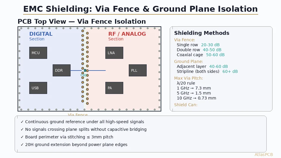
Shielding Techniques
When design techniques alone cannot achieve compliance, shielding provides additional attenuation:
PCB-Level Shielding
- Ground pour on outer layers: Fill unused areas of signal layers with copper connected to ground. This reduces the antenna efficiency of traces near the board edge.
- Via fencing: A row of ground vias around sensitive circuits or along board edges creates a partial Faraday cage. Space vias at λ/20 intervals for the highest frequency of concern.
- Board-level shield cans: Metal enclosures soldered directly to the PCB over noisy circuits (clock generators, wireless modules) provide 20–40 dB of additional shielding.
Enclosure Shielding
- Ensure good electrical contact between the PCB ground and enclosure at all connector locations
- Use conductive gaskets at enclosure seams if gaps exceed λ/20 at the highest EMI frequency
- Ground the cable shields to the enclosure (not the PCB ground) at the connector entry point
EMI Compliance Test Preparation
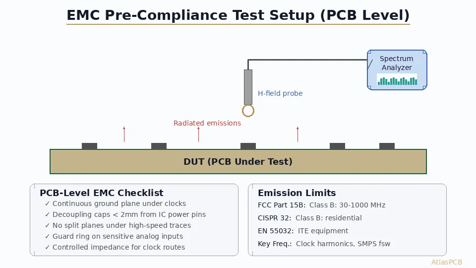
Pre-Compliance Testing
Before formal compliance testing (which can cost $5,000–$15,000 per session), perform pre-compliance measurements:
Near-field probing: Use H-field and E-field near-field probes connected to a spectrum analyzer to identify the hottest EMI sources on the board. This localizes problems before they become expensive.
Current probe on cables: Clamp a current probe on each cable and measure common-mode current. The FCC/CISPR radiated emission limits can be estimated from the common-mode cable current.
Conducted emissions scan: Measure power line conducted emissions with a LISN (Line Impedance Stabilization Network) and spectrum analyzer.
Common EMI Failure Frequencies and Causes
| Frequency Pattern | Likely Source | Investigation Priority |
|---|---|---|
| Harmonics of clock frequency | Clock oscillator, clock distribution | Check clock trace routing, add series R |
| Harmonics of switching regulator | DC-DC converter | Check input/output filtering, loop area |
| Broadband noise floor elevation | High-speed bus (DDR, USB 3.x) | Check return path continuity, decoupling |
| Single frequency spike | Crystal oscillator, PLL | Check oscillator grounding, shield can |
| Noise at cable resonance | I/O cable acting as antenna | Add common-mode choke, improve cable shielding |
EMI Design Checklist
Use this checklist during design review to catch common EMI issues:
Grounding:
- Continuous ground plane under all high-speed signals
- No splits or slots in ground plane under signal traces
- Ground plane stitching vias at ≤λ/20 spacing
- Single-point or controlled connection between analog and digital grounds
Decoupling:
- Decoupling capacitors within 2 mm of every IC power pin
- Multiple capacitor values for broadband coverage
- Short, wide traces from cap to pin (or direct via connection)
- Bulk capacitor at power entry
Filtering:
- Common-mode chokes on all external cables
- Pi-filter on power input
- Ferrite beads on internal power rails to sensitive circuits
- ESD protection on all external interfaces
Layout:
- Functional zoning (digital, analog, power, I/O)
- Connectors grouped on one edge
- High-speed traces 3× H from board edge
- Clock traces minimized in length and shielded
- Series termination on high-speed outputs
Stackup:
- Signal-ground-signal layer ordering (every signal has adjacent reference plane)
- Thin dielectric between signal and ground (tight coupling)
- Adjacent signal layers routed orthogonally
Conclusion
EMI compliance is a design discipline, not a testing exercise. The techniques described in this guide — continuous ground planes, disciplined decoupling, I/O filtering, strategic component placement, and edge rate management — represent decades of accumulated engineering wisdom. Applied systematically from the start of the design process, they dramatically increase the probability of first-pass compliance.
The most expensive EMI fix is the one applied after production tooling is complete. Invest the time upfront in proper PCB design for EMI compliance, and your products will reach market faster with fewer costly redesign cycles.
For a deeper exploration of EMC and EMI principles at the board level, visit our [EMC/EMI PCB design guide]/blog/emc-emi-pcb-design/). And when you’re ready to fabricate, request a quote from Atlas PCB — our controlled-impedance manufacturing and quality processes support your compliance objectives.
Further Reading
- [mmWave PCB Material Selection: Rogers vs Megtron vs LCP for 5G and 6G Applications]/blog/mmwave-pcb-material-selection-rogers-megtron-lcp-5g-6g/)
- [Rogers PCB Fabrication: Material Sourcing, Lead Times & Quality Control]/blog/rogers-pcb-fabrication/)
- [HDI PCB Design for 5G Antenna Integration: Signal Integrity Challenges in Millimeter-Wave Applications]/blog/hdi-5g-antenna-integration-pcb-design/)
- [RF PCB Material Selection for Automotive Radar: Rogers vs PTFE Performance Analysis at 77-81 GHz]/blog/automotive-radar-pcb-materials-rogers-ptfe-analysis/)
- [ENEPIG vs ENIG Surface Finish: Complete Comparison for Wire Bonding, Solderability, and Long-Term Reliability]/blog/enepig-vs-enig-surface-finish-wire-bonding/)
- High-Frequency RF PCB Services
About AtlasPCB — We specialize in complex PCB manufacturing for HDI, RF, and high-reliability applications. Explore our RF and high-frequency PCB services, or get an impedance-controlled PCB manufacturing . Every order includes free engineering review. Get your quote.
Reviewed by AtlasPCB Engineering Team — IPC-certified manufacturing specialists with 15+ years of production experience in HDI, RF, and high-reliability PCB fabrication. Content based on factory floor data and real customer design reviews.
- emi compliance
- emc design
- pcb layout
- electromagnetic interference
- radiated emissions