· AtlasPCB Engineering · Engineering · 11 min read
What Causes PCB Delamination? Root Causes, Prevention, and Quality Control
Understand the root causes of PCB delamination including moisture absorption, thermal stress, and material incompatibility. Learn prevention strategies, IPC inspection standards, and manufacturing process controls.
Delamination is one of the most serious reliability defects in printed circuit board manufacturing. When layers of a PCB separate from each other — whether laminate from laminate, copper from substrate, or prepreg from core — the board’s structural integrity is compromised, impedance values shift unpredictably, and the risk of field failure increases dramatically.
Unlike many PCB defects that are immediately apparent, delamination can be latent — invisible during initial inspection but manifesting after thermal cycling, reflow soldering, or extended service life. This makes understanding its root causes and implementing prevention strategies essential for any product that demands reliability.
What Is PCB Delamination?
Delamination is the physical separation between bonded layers in a multilayer PCB. It can occur at several interfaces:
- Prepreg-to-core: The semi-cured prepreg resin fails to bond properly to the cured core laminate
- Copper-to-laminate: The copper foil separates from the underlying or overlying dielectric
- Prepreg-to-copper (inner layer): Internal copper planes or traces lose adhesion to the prepreg
- Within the prepreg layer itself: Cohesive failure of the resin system
Delamination appears visually as:
- Blisters: Raised, bubble-like areas on the board surface
- Measling: White spots or crosses within the laminate at glass fiber intersections (technically a prelude to delamination)
- Weave exposure: Visible glass fiber pattern where resin has separated from the weave
- Internal voids: Visible only through cross-section or acoustic imaging
Delamination vs. Related Defects
| Defect | Description | Key Difference from Delamination |
|---|---|---|
| Delamination | Layer separation at interface | Occurs between bonded surfaces |
| Measling | White spots at glass fiber intersections | Resin fracture, often precursor to delamination |
| Blistering | Localized swelling on surface | May be caused by delamination or trapped gas |
| Crazing | Network of fine cracks in resin | Resin failure without layer separation |
| Haloing | White ring around drilled holes | Mechanical damage to resin from drilling |
Root Causes of PCB Delamination
1. Moisture Absorption and Outgassing
This is the #1 cause of delamination in production environments.
PCB laminates are hygroscopic — they absorb moisture from the atmosphere during storage and processing. Standard FR-4 can absorb up to 0.15% moisture by weight, and even high-Tg materials absorb 0.08–0.12%.
When the board is subjected to high temperatures during:
- Reflow soldering (peak 250–260°C for lead-free)
- Wave soldering (250°C)
- Hot air leveling (HASL, 260°C)
- Rework operations
The absorbed moisture rapidly converts to steam, expanding with enormous pressure (up to 40 psi at 260°C). This pressure exceeds the bond strength between layers, forcing them apart.
Critical factors:
- Moisture content above 0.1% by weight significantly increases delamination risk at lead-free reflow temperatures
- Exposure to humidity above 50% RH for more than 8 hours requires pre-baking before thermal processing
- Thicker boards (>2.0 mm) are more susceptible because moisture penetrates deeper and has fewer escape paths
| Board Thickness | Pre-Bake Requirement | Bake Temperature | Bake Duration |
|---|---|---|---|
| <1.0 mm | If stored >48h at >50% RH | 105–120°C | 2–4 hours |
| 1.0–2.0 mm | If stored >24h at >50% RH | 105–120°C | 4–6 hours |
| 2.0–3.0 mm | If stored >12h at >50% RH | 105–120°C | 6–8 hours |
| >3.0 mm | If stored >8h at >50% RH | 105–120°C | 8–16 hours |
2. Thermal Stress Exceeding Material Limits
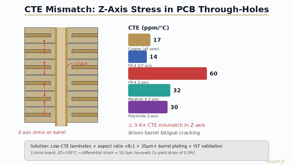
Every laminate material has a glass transition temperature (Tg) above which the resin transitions from a rigid, glassy state to a soft, rubbery state. Above Tg, the Z-axis CTE increases dramatically (typically 3–5× the below-Tg value), and the resin’s mechanical strength drops.
| Material | Tg (DSC) | Td (5% weight loss) | Z-CTE below Tg | Z-CTE above Tg |
|---|---|---|---|---|
| Standard FR-4 | 130–140°C | 310°C | 50 ppm/°C | 250 ppm/°C |
| Mid-Tg FR-4 | 150–160°C | 325°C | 45 ppm/°C | 200 ppm/°C |
| High-Tg FR-4 | 170–180°C | 340°C | 40 ppm/°C | 180 ppm/°C |
| Very High-Tg | >200°C | >350°C | 35 ppm/°C | 150 ppm/°C |
| Polyimide | 250°C+ | >400°C | 30 ppm/°C | 100 ppm/°C |
Lead-free soldering impact: The transition from tin-lead (183°C peak) to lead-free solder (250–260°C peak) was a watershed moment for delamination. The 70–80°C higher peak temperature means the board spends more time above Tg, with significantly higher Z-axis expansion. Standard Tg FR-4 (130°C) is marginal for lead-free processes — high-Tg material (170°C+) is strongly recommended.
For a deep dive into high-Tg material selection, see our [high-Tg PCB material selection guide]/blog/high-tg-pcb-material-selection/).
3. Inadequate Lamination Process
The lamination press cycle is where the multilayer PCB is actually created — prepreg resin melts, flows, and cures to bond the layers together. Deficiencies in this process directly cause delamination:
Insufficient pressure: If lamination pressure is too low, the prepreg resin may not adequately wet the copper surfaces or fill the spaces between circuit features, leaving voids that become delamination initiation sites.
Incorrect temperature profile:
- Ramp rate too fast → uneven resin flow, trapped air
- Peak temperature too low → incomplete cure, weak bond
- Peak temperature too high → resin degradation, brittleness
- Cure time too short → under-cured resin with poor mechanical properties
Press variability: Temperature and pressure variations across the press platen can create localized areas of poor bonding. This is especially problematic for large panels where edge-to-center temperature differences can be significant.
4. Contamination at Layer Interfaces
Any contamination between bonded surfaces compromises adhesion:
| Contaminant | Source | Effect |
|---|---|---|
| Oxide residue | Incomplete oxide treatment or over-etching | Weak copper-to-resin bond |
| Fingerprints / oils | Handling without gloves | Localized adhesion failure |
| Dust / particles | Cleanroom deficiency | Void formation at interface |
| Chemical residue | Incomplete rinsing after processing | Resin won’t wet surface properly |
| Oxidized copper | Extended storage between inner layer processing and lamination | Reduced peel strength |
Brown oxide vs. black oxide: The surface treatment applied to inner-layer copper before lamination is critical. Black oxide processes create a microscopically rough copper surface for mechanical adhesion, while alternative (reduced oxide) treatments provide chemical bonding. Both must be properly controlled — over-processing creates a fragile oxide that fractures under stress, while under-processing provides insufficient adhesion.
5. Material Incompatibility
Not all PCB materials are compatible with each other in hybrid stackups:
- CTE mismatch: Materials with significantly different thermal expansion rates create shear stress at their interface during temperature cycling. Over many cycles, this stress fatigues the bond.
- Resin system incompatibility: Mixing different resin systems (e.g., standard FR-4 prepreg with a polyimide core) can result in poor cross-linking at the interface.
- Copper foil type mismatch: Some high-frequency materials require specific copper foil treatments for adequate adhesion. Using standard ED copper where the material specifies rolled annealed copper can cause premature delamination.
For guidance on selecting compatible material combinations, see our [PCB material selection guide]/blog/pcb-material-selection-guide/).

Consequences of Delamination
Delamination is not merely a cosmetic defect — it has serious functional and reliability implications:
Electrical Consequences
| Impact | Mechanism | Severity |
|---|---|---|
| Impedance change | Air gap between layers changes effective Dk | Signal integrity degradation |
| Open circuits | Via barrel or inner-layer connection fractures | Complete circuit failure |
| Intermittent connections | Delamination opens/closes with temperature cycling | Extremely difficult to diagnose |
| Increased crosstalk | Delamination changes coupling between layers | Increased noise in adjacent circuits |
| Reduced insulation resistance | Moisture ingress into delaminated area | Potential short circuit over time |
Mechanical Consequences
- Progressive failure: Delamination tends to propagate — once initiated, thermal and mechanical cycling extends the delaminated area
- Reduced flexural strength: Delaminated boards are significantly weaker and more susceptible to cracking
- Assembly damage: Delaminated areas near component pads can cause tombstoning, lifted pads, or solder joint failure during assembly
Reliability Consequences
In field applications, delamination is a time bomb. It may not cause immediate failure, but:
- Moisture enters the delaminated cavity, accelerating corrosion of internal copper
- Thermal cycling progressively extends the delamination
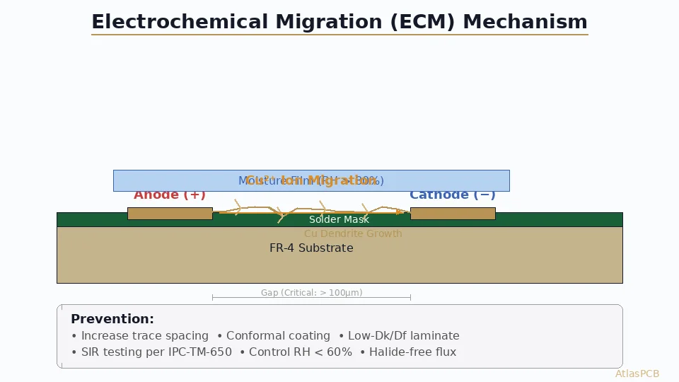
- Conductive anodic filament (CAF) growth is greatly accelerated in delaminated areas, potentially causing short circuits between conductors
Prevention Strategies
Material Selection
Choose appropriate Tg for the thermal profile. For lead-free assembly:
- Standard Tg (130°C): Suitable only for tin-lead solder
- Mid-Tg (150°C): Marginal for lead-free, acceptable for single reflow
- High-Tg (170°C+): Recommended for lead-free, multiple reflows
- Very high-Tg (200°C+) or polyimide: Required for extreme thermal demands
Match materials within the stackup. Use prepreg and core from the same material system. Consult the laminate manufacturer’s compatibility guide before creating hybrid stackups.
Specify low-moisture-absorption materials for applications exposed to humid environments (outdoor, automotive, marine).
Design Practices
Balanced copper distribution: Large areas of copper on one side with minimal copper on the other create differential resin flow during lamination and differential CTE stress. Balance copper coverage across the board and between adjacent layers.
Adequate copper-free zones: Allow sufficient resin-to-resin bonding areas. Boards with 90%+ copper coverage on inner layers have reduced delamination margin because the bond is primarily copper-to-resin (typically weaker than resin-to-resin).
Thermal relief pads on inner planes: Solid connections to large copper planes act as heat sinks during soldering, creating localized thermal stress. Thermal relief connections distribute the stress.
Avoid very thick boards without justification: Boards thicker than 3.0 mm are inherently more susceptible to delamination due to higher Z-axis expansion and greater moisture absorption capacity.
Manufacturing Process Controls
Incoming material control:
- Store laminates in climate-controlled conditions (23 ±3°C, <50% RH)
- Track material age — use FIFO (first-in, first-out) rotation
- Pre-bake materials that have been exposed to uncontrolled conditions
- Verify Tg and Td of incoming material lots
Inner layer processing:
- Apply oxide treatment within 24 hours of etching
- Verify oxide color, thickness, and adhesion before lamination
- Handle with lint-free gloves in a cleanroom environment
- Complete lamination within 48 hours of oxide treatment
Lamination press control:
- Monitor and record temperature at multiple points across the platen
- Verify pressure uniformity (±5% across the press)
- Follow the laminate manufacturer’s recommended press cycle exactly
- Validate cure completion through DSC (Differential Scanning Calorimetry) on sample coupons
Post-lamination handling:
- Bake boards within 8 hours before any thermal process if stored >24 hours
- Minimize time between lamination and subsequent processing
- Store finished boards in moisture-barrier bags with desiccant for shipment
IPC Inspection Standards and Acceptance Criteria
IPC-6012 Delamination Criteria
IPC-6012 defines three classes of PCBs with progressively stricter requirements:
| Criterion | Class 1 (General) | Class 2 (Dedicated Service) | Class 3 (High Reliability) |
|---|---|---|---|
| Surface delamination | Acceptable if doesn’t reduce spacing below minimum | Blister ≤ per specimen area limit | Not acceptable |
| Internal delamination | Acceptable if doesn’t reduce spacing | ≤ specified area limit per coupon | Not acceptable |
| Post thermal stress | Must survive 1 cycle at 288°C/10s | Must survive 3 cycles at 288°C/10s | Must survive 6 cycles at 288°C/10s |
| Measling | Acceptable | Limited per IPC-A-600 | Minimal, no degradation of spacing |
Key Test Methods
IPC-TM-650 Method 2.6.8 — Thermal Stress: The board (or coupon) is floated on molten solder at 288°C for 10 seconds, then inspected for delamination via cross-section. This simulates the thermal shock of wave soldering or reflow.
IPC-TM-650 Method 2.1.1 — Microsectioning: The board is cross-sectioned, polished, and examined under a microscope at 50–200× magnification. This reveals internal delamination, measling, void content, and resin recession.
IPC-TM-650 Method 2.6.16 — Moisture and Insulation Resistance: The board is subjected to humidity exposure (85°C/85% RH for 96 hours) followed by insulation resistance measurement. Delamination accelerates moisture ingress, which reduces insulation resistance.
Acceptance Testing Recommendations
| Application | Recommended Testing | Frequency |
|---|---|---|
| Consumer electronics | Visual + thermal stress (1 cycle) | Sample per lot |
| Industrial / telecom | Visual + thermal stress (3 cycles) + microsection | Every lot |
| Automotive | Visual + thermal stress (6 cycles) + microsection + IST | Every lot |
| Aerospace / military | Full IPC-6012 Class 3 + humidity + C-SAM | 100% inspection |
| Medical implant | Full Class 3 + extended humidity + burn-in | 100% + destructive sample |
For a comprehensive overview of PCB reliability testing methods, see our [PCB reliability testing guide]/blog/pcb-reliability-testing/).
Troubleshooting Delamination in Production
When delamination is found during production, systematic root cause analysis is essential:
Step 1: Characterize the Failure
- Location: Surface or internal? Near vias, edges, or random?
- Distribution: Random (process variable) or systematic (design/material)?
- Timing: At which process step does delamination first appear?
- Interface: Which layers are separating? (This identifies the failing bond.)
Step 2: Investigate by Failure Mode
| Failure Location | Most Likely Cause | Investigation Focus |
|---|---|---|
| Surface blister after reflow | Moisture + thermal stress | Check pre-bake, material storage |
| Internal delamination near vias | Z-axis CTE stress | Check Tg, thermal profile, via design |
| Inner-layer separation, random | Lamination process | Check press parameters, oxide treatment |
| Inner-layer separation, systematic | Material contamination | Check handling, cleanroom, chemical baths |
| Edge delamination | Incomplete resin cure at edges | Check lamination pressure uniformity |
| Post-assembly delamination | Multiple reflow cycles | Check material Tg vs. thermal budget |
Step 3: Corrective Actions
Immediate:
- Bake affected inventory before further thermal processing
- Increase inspection sampling rate
- Quarantine suspect material lots
Short-term:
- Adjust lamination parameters (verify with cure monitoring)
- Improve oxide treatment process controls
- Reduce thermal profile peak temperature (if possible within solder specifications)
Long-term:
- Upgrade to higher-Tg material if the current material is marginal
- Implement moisture management program (sealed storage, pre-bake protocols)
- Add thermal stress testing as incoming inspection for multilayer boards
- Review and tighten lamination press maintenance schedule
Conclusion
PCB delamination is a multifaceted problem with roots in material science, process engineering, and design choices. The shift to lead-free soldering has made it more prevalent and more critical to address, as the higher thermal demands push conventional materials closer to their limits.
Prevention is always more effective and economical than detection and correction. By selecting appropriate materials for the thermal profile, maintaining strict moisture management, controlling the lamination process with data-driven parameters, and testing to IPC standards, you can virtually eliminate delamination from your production.
The key takeaway: delamination is rarely caused by a single factor. It typically results from the combination of marginal material selection, inadequate moisture control, and aggressive thermal profiles. Address all three, and your boards will maintain their structural and electrical integrity through manufacturing, assembly, and years of service.
Need high-reliability PCBs manufactured with rigorous delamination prevention? Request a quote from Atlas PCB — our quality processes, material management, and IPC-certified inspection ensure your boards meet the most demanding reliability requirements.
Further Reading
- [AI Hardware PCB Thermal Management: Advanced Multilayer Stackup Design for 1000W+ Processing Units]/blog/ai-hardware-pcb-thermal-management-multilayer-design/)
- [PCB Warpage Control: Causes, IPC Limits, and Prevention in Multilayer Boards]/blog/pcb-warpage-control-multilayer/)
- [Rogers PCB Fabrication: Material Sourcing, Lead Times & Quality Control]/blog/rogers-pcb-fabrication/)
- [PCB Rigid-Flex Bend Zone Reliability: Design Rules, Material Selection & Lifecycle Testing]/blog/pcb-rigid-flex-bend-zone-reliability/)
- [ENEPIG vs ENIG Surface Finish: Complete Comparison for Wire Bonding, Solderability, and Long-Term Reliability]/blog/enepig-vs-enig-surface-finish-wire-bonding/)
- Our Manufacturing Capabilities
About AtlasPCB — We specialize in complex PCB manufacturing for HDI, RF, and high-reliability applications. Explore our full PCB manufacturing capabilities . Every order includes free engineering review. Get your quote.
Reviewed by AtlasPCB Engineering Team — IPC-certified manufacturing specialists with 15+ years of production experience in HDI, RF, and high-reliability PCB fabrication. Content based on factory floor data and real customer design reviews.
- pcb delamination
- pcb reliability
- manufacturing defect
- ipc standards
- lamination quality