· AtlasPCB Engineering · Engineering · 11 min read
5G Antenna PCB Fabrication: mmWave Array Design and Manufacturing Challenges
Building 5G mmWave antenna arrays demands PCB fabrication precision most shops cannot deliver. Learn the material selection, stackup design, etching tolerances, and manufacturing process requirements for 24-40 GHz antenna PCBs.
Quick Reference: 5G mmWave Antenna PCB Specifications
| Parameter | n257 (28 GHz) | n258 (26 GHz) | n260 (39 GHz) | n261 (28 GHz) |
|---|---|---|---|---|
| Center freq | 27.5 GHz | 25.875 GHz | 38.5 GHz | 27.925 GHz |
| Bandwidth | 3 GHz | 3.25 GHz | 2 GHz | 0.85 GHz |
| Patch size (RO4350B, 10mil) | 3.2 x 3.2 mm | 3.4 x 3.4 mm | 2.2 x 2.2 mm | 3.2 x 3.2 mm |
| Element spacing (lambda/2) | 5.4 mm | 5.8 mm | 3.9 mm | 5.4 mm |
| Substrate recommendation | Rogers RO4350B | Rogers RO4350B | Rogers RO3003 / PTFE | Rogers RO4350B |
| Min etch tolerance | +/-0.5 mil | +/-0.5 mil | +/-0.3 mil | +/-0.5 mil |
| Typical array size | 4x4 or 8x8 | 4x4 or 8x8 | 8x8 or 16x16 | 4x4 |
At millimeter-wave frequencies, the PCB is not merely an interconnect carrier — it is the antenna itself. Every manufacturing tolerance directly affects radiation pattern, gain, and impedance matching.
Why mmWave Antenna PCB Fabrication Is Different from Standard RF
Most RF PCB work operates in the 1-10 GHz range where material properties are forgiving and manufacturing tolerances have moderate impact on performance. The jump to mmWave (24+ GHz) changes the engineering equation fundamentally because wavelengths shrink below the scale of manufacturing variability.
At 28 GHz, a wavelength in RO4350B substrate is approximately 5.8mm. The patch antenna element is half a guided wavelength — roughly 3.2mm square. A mere 25 microns (1 mil) of etch variation shifts the patch resonant frequency by approximately 140 MHz, which is 5% of a 3 GHz bandwidth. While individual patches can tolerate some frequency shift, an array of 16 or 64 elements with random etch variation produces unpredictable beam squinting and gain degradation.
In our facility, mmWave antenna boards run on a dedicated fine-line etching process with modified spray pressures, optimized DES (Develop-Etch-Strip) chemistry concentration, and 100% optical inspection of patch dimensions post-etch. Standard PCB fabrication processes that achieve +/-1.5 mil etch tolerance are inadequate — we hold +/-0.5 mil on antenna features, which is tighter than most HDI trace/space specifications.
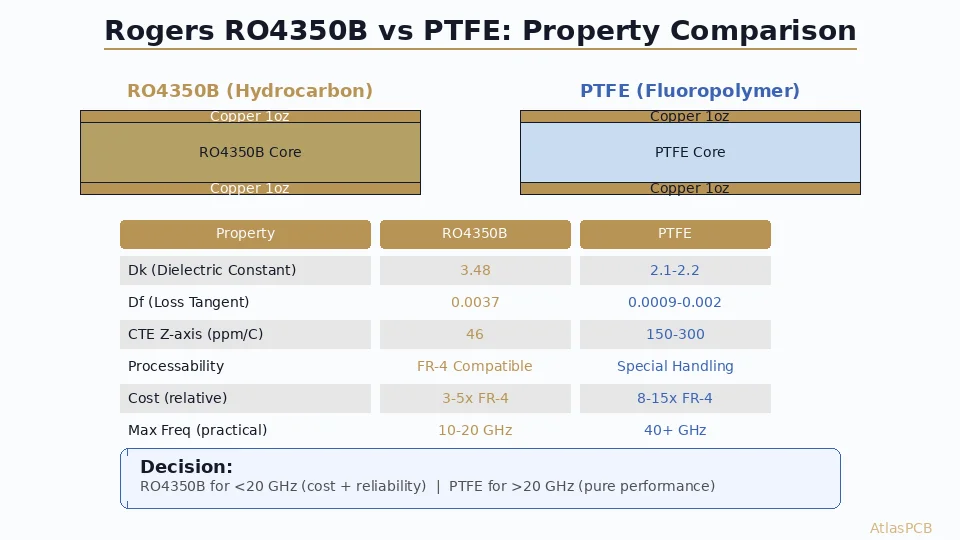
The substrate itself introduces additional constraints. Rogers RO4350B has a specified Dk tolerance of +/-0.05 at 10 GHz. At 28 GHz, the effective Dk shifts slightly due to the Dk-vs-frequency characteristic, and the +/-0.05 tolerance becomes a meaningful source of patch frequency offset. Selecting from a single material lot — where all panels have matching Dk within +/-0.02 — is standard practice for antenna array production.
CHINA RF PCB MANUFACTURER
5G mmWave Antenna PCB Fabrication
We maintain dedicated fine-line etching processes for mmWave antenna arrays. +/-0.5 mil etch tolerance, lot-matched Rogers material, and 100% patch dimension verification.
Get RF Quote ›Stackup Architecture for 5G Antenna Modules
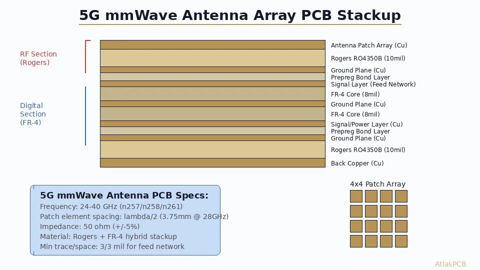
The Hybrid RF/Digital Approach
Modern 5G antenna modules integrate the antenna array, beamforming IC, power management, and digital control into a single PCB assembly. This demands a stackup that serves both mmWave RF performance (low loss, tight impedance) and digital routing density (fine trace/space, multiple signal layers). The standard approach is a hybrid material stackup.
A typical 8-layer 5G antenna module stackup:
| Layer | Function | Material | Thickness |
|---|---|---|---|
| L1 | Antenna patches | Cu on Rogers RO4350B | 0.5oz Cu |
| Core 1 | Antenna substrate | Rogers RO4350B | 10 mil |
| L2 | Ground plane (antenna reference) | Cu | 1oz |
| PP 1 | Bonding | Rogers 4450F prepreg | 4 mil |
| L3 | RF feed network | Cu | 0.5oz |
| Core 2 | RF routing substrate | Rogers RO4350B or FR-4 | 8 mil |
| L4 | Ground plane | Cu | 1oz |
| PP 2 | Transition prepreg | FR-4 compatible prepreg | 4 mil |
| L5 | Digital signal layer | Cu | 1oz |
| Core 3 | Digital substrate | FR-4 (High-Tg) | 8 mil |
| L6 | Power/Ground plane | Cu | 1oz |
| PP 3 | Bonding | FR-4 prepreg | 4 mil |
| L7 | Digital signal layer | Cu | 1oz |
| Core 4 | Digital substrate | FR-4 (High-Tg) | 8 mil |
| L8 | Component/Power layer | Cu | 1oz |
The critical design decisions in this stackup are: (1) the antenna substrate thickness determines bandwidth and efficiency, (2) the ground plane directly beneath the patches must be continuous with no apertures under the array area, and (3) the RF-to-digital transition must use a compatible bonding prepreg that survives thermal cycling without delamination.
Substrate Thickness and Antenna Performance
The relationship between substrate thickness and antenna bandwidth is roughly: thicker substrate equals wider bandwidth but lower efficiency due to surface wave excitation. For 28 GHz n257 band (3 GHz bandwidth, ~10.9% fractional bandwidth), a 10-mil (0.254mm) RO4350B substrate provides approximately 8-12% impedance bandwidth, which is borderline. Many designs use dual-resonance techniques (stacked patches or slot coupling) to extend bandwidth beyond what a single patch on 10-mil substrate can achieve.
At 39 GHz (n260), the required substrate thickness drops to 6-8 mil for single-patch designs, creating handling challenges during fabrication. These thinner substrates are more susceptible to warpage during lamination and etching, requiring specialized panel support fixtures.
Critical Manufacturing Challenges
Challenge 1: Patch Dimensional Control
The most critical manufacturing parameter for mmWave antenna PCBs is patch dimension accuracy. Unlike trace width variation (which primarily affects impedance), patch dimension variation directly shifts the resonant frequency of each antenna element.
For a 4x4 element array at 28 GHz, if each element has a random frequency offset due to etch variation, the array’s composite radiation pattern degrades. Specifically:
- +/-0.5 mil etch tolerance → +/-140 MHz per element (acceptable for n257’s 3 GHz bandwidth)
- +/-1.0 mil etch tolerance → +/-280 MHz per element (marginal)
- +/-1.5 mil etch tolerance → +/-420 MHz per element (unacceptable — gain drops 1-2 dB)
Our process achieves +/-0.5 mil on antenna features through modified etching parameters: reduced spray pressure to minimize undercut variation, tighter developer concentration control (+/-0.2% vs standard +/-0.5%), and breakpoint detection during etch to avoid over-etching thin features.
Challenge 2: Copper Surface Roughness
At mmWave frequencies, current flow concentrates in the top 1-2 skin depths of the conductor (skin depth at 28 GHz in copper is approximately 0.4 microns). Surface roughness on the same scale as skin depth increases effective conductor length, directly increasing loss. Standard rolled or electrodeposited copper foil has RMS roughness of 1-3 microns — comparable to or exceeding the skin depth.
For antenna applications where every 0.1 dB of loss matters, low-profile copper foils (LP, VLP, or HVLP grades with 0.5-1.5 um roughness) provide measurable improvement. The tradeoff is adhesion — smoother copper bonds less strongly to the laminate, creating reliability concerns. Rogers addresses this with their proprietary bonding technology on certain laminate grades.
In our production, we stock Rogers materials with standard (ED) and low-profile (VLP) copper options. For 28 GHz designs where the feed network exceeds 2 inches total, we typically recommend VLP copper despite the 10-15% material cost premium, because the loss reduction (0.3-0.5 dB/inch improvement at 28 GHz) provides substantial system-level benefit.
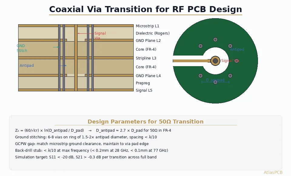
Challenge 3: Via Transitions in mmWave Feed Networks
The feed network connecting the beamforming IC to the antenna array must transition between PCB layers — typically from a buried feed layer (L3) through a ground plane (L2) to the antenna patches (L1). At mmWave frequencies, via transitions radiate and introduce impedance discontinuities if not properly designed and manufactured.
Key manufacturing parameters for mmWave via transitions:
- Via pad size and clearance: Must be tightly controlled to maintain characteristic impedance through the transition. A via pad 2 mil larger than designed shifts impedance by 3-5 ohms at 28 GHz.
- Anti-pad concentricity: The clearance hole in the ground plane must be concentric with the via within +/-1 mil; offset creates asymmetric field coupling and mode conversion.
- Backdrilling: Via stubs extending below the target layer create resonances. At 28 GHz, a 10-mil stub resonates at approximately 75 GHz — outside the passband but within the mixer spurious range for some architectures. Backdrilling accuracy of +/-3 mil is our standard specification.
RF PCB DESIGN AND MANUFACTURING
From Schematic to mmWave Antenna Hardware
Our process engineers work with your RF team on stackup optimization, material selection, and via transition design before fabrication begins. First-pass success rate above 92% on 5G antenna boards.
Testing and Qualification for 5G Antenna PCBs
Electrical Verification
Standard electrical testing (continuity and isolation) is necessary but insufficient for antenna PCBs. Additional verification includes:
- Impedance measurement (TDR): Feed network impedance verified at coupon level for every production lot. Target 50 ohms +/-5%.
- Insertion loss measurement: Stripline test coupons on the same panel measured at 28 GHz to verify material and process meet loss specifications.
- Patch dimension inspection: Automated optical inspection (AOI) configured to measure patch element dimensions against +/-0.5 mil tolerance.
Reliability Testing
5G infrastructure antenna PCBs must survive 20+ year outdoor deployment with thermal cycling from -40 to +85C. Key qualification tests include:
- Thermal cycling (IPC-TM-650, Method 2.6.7.2): 500-1000 cycles, -40 to +125C
- Humidity exposure (85C/85% RH): 1000 hours minimum
- CAF (Conductive Anodic Filament) testing: Critical for hybrid stackups where moisture ingress at material interfaces can create conductive paths
- Peel strength (IPC-TM-650, Method 2.4.8): Verify copper adhesion exceeds 4 lb/inch after thermal stress, particularly at Rogers-to-prepreg interfaces
In our experience, the most common qualification failure on hybrid 5G antenna boards is delamination at the Rogers-to-FR-4 bonding interface after extended thermal cycling. Proper prepreg selection (Rogers 4450F or proven compatible) and optimized lamination profiles are essential. We run thermal cycling qualification on every new hybrid stackup configuration before approving it for production.
Design Guidelines for Manufacturability
Based on our production experience with 5G antenna PCBs, these design choices maximize first-pass success:
- Keep antenna substrate at 10 mil standard thickness — 8-mil and 6-mil substrates significantly increase handling difficulty and warp risk
- Use 4x4 or 8x8 arrays — larger arrays increase dimensional tolerance impact; if you need 16x16, consider tiled sub-arrays
- Place beamforming IC on opposite side from antenna array — eliminates routing congestion under patch elements
- Maintain 3x-wavelength continuous ground under array — no ground plane cutouts, vias, or power splits within the antenna ground reference area
- Consolidate feed network via sizes — use a single via diameter for all feed transitions to maintain consistent impedance
- Add 5G test coupons to panel border — insertion loss stripline, TDR coupon, and patch dimension verification elements
ROGERS PCB MANUFACTURER
Rogers Material In Stock — 5-Day Standard Lead Time
We stock RO4350B (10, 20, 30 mil), RO4003C, and RO3003. Hybrid Rogers/FR-4 stackups are our specialty — over 200 unique designs delivered in Q2 2026 alone.
Check Material Availability ›Summary: What Your 5G Antenna PCB Fabricator Must Deliver
Choosing a fabricator for 5G mmWave antenna PCBs requires verifying specific capabilities that most standard shops lack:
| Capability | Minimum Requirement | What to Ask |
|---|---|---|
| Etch tolerance | +/-0.5 mil on antenna features | ”What is your etch tolerance on Rogers material?” |
| Rogers processing | Full compatibility, in-house experience | ”How many Rogers antenna boards/month do you produce?” |
| Hybrid stackups | Proven Rogers + FR-4 bonding | ”Which prepreg do you use at Rogers-to-FR-4 interface?” |
| Copper roughness options | VLP or LP copper available | ”Can you source RO4350B with VLP copper?” |
| Impedance control at 28 GHz | TDR + insertion loss test coupons | ”Do you provide RF coupon data with antenna boards?” |
| Backdrilling | +/-3 mil depth accuracy | ”What is your backdrilling depth tolerance?” |
The 5G antenna PCB is one of the most demanding applications in commercial PCB manufacturing today — combining the material requirements of aerospace radar with the cost sensitivity of consumer electronics. Selecting the right fabrication partner at the design stage, not after prototyping problems emerge, is the single most important decision for program schedule success.
ATLASPCB
Building 5G Antenna Hardware? Let's Talk Stackup.
Upload your antenna array design or describe your requirements. We provide material recommendations, stackup optimization, and rapid prototyping for mmWave PCBs.
Start Your 5G PCB Project ›Reviewed by AtlasPCB Engineering Team — 15+ years in advanced PCB fabrication for RF, HDI, and rigid-flex applications.
Related Reading:
About AtlasPCB — We specialize in complex PCB manufacturing for HDI, RF, and high-reliability applications. Explore our RF and high-frequency PCB services . Every order includes free engineering review. Get your quote.
Reviewed by AtlasPCB Engineering Team — IPC-certified manufacturing specialists with 15+ years of production experience in HDI, RF, and high-reliability PCB fabrication. Content based on factory floor data and real customer design reviews.
- 5G antenna PCB
- mmWave
- PCB fabrication
- Rogers RO4350B
- RF PCB
- antenna array
- phased array