· AtlasPCB Engineering · Engineering · 8 min read
PCB Bow and Twist: IPC-TM-650 Measurement Methods, Causes, and Prevention Strategies
Understand PCB bow and twist according to IPC-TM-650 standards, learn measurement techniques, root causes in lamination and copper distribution, and proven prevention methods for SMT-compatible flatness.

What Are Bow and Twist in PCB Manufacturing?
Flatness is a critical quality parameter for printed circuit boards, particularly those destined for automated surface mount assembly. When a PCB deviates from perfect flatness, the deformation is classified as either bow or twist — two distinct failure modes with different root causes and different remediation strategies.
Understanding the difference matters because:
- SMT pick-and-place machines have limited tolerance for board non-flatness
- BGA and QFN packages require coplanarity to achieve reliable solder joints
- Wave soldering fixtures assume predictable board shape
- Connectors and press-fit pins require mechanical precision
A board that exceeds flatness limits can cause:
- Solder paste bridging or insufficient paste transfer during stencil printing
- Component placement errors and head crashes on pick-and-place machines
- Open solder joints under BGA packages
- Fixture fit failures in test and assembly
IPC-TM-650 Measurement Methods
IPC-TM-650 Section 2.4.22 defines the standard test method for measuring bow and twist. Understanding these methods is essential for both designers who specify flatness requirements and fabricators who must verify compliance.
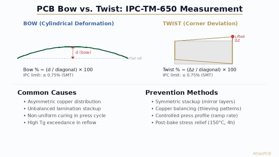
Measuring Bow
Bow is a cylindrical or spherical curvature — the board curves uniformly like a shallow bowl or trough.
Measurement procedure:
- Place the board concave side up on a flat reference surface (granite surface plate)
- Using a straightedge placed along the board’s diagonal, measure the maximum distance between the board surface and the straightedge
- This maximum gap distance is the bow height (d)
- Calculate:
Bow % = (d / diagonal length) × 100
Example: A 200 mm × 150 mm board (diagonal = 250 mm) with 1.5 mm maximum deflection has bow = (1.5/250) × 100 = 0.6% — within the 0.75% SMT limit.
Measuring Twist
Twist is a non-planar deformation — think of holding a board by two diagonally opposite corners and seeing the other two corners lift.
Measurement procedure:
- Place the board on a flat surface — three corners will touch while one lifts
- Measure the height of the lifted corner above the reference surface — this is Δz
- Calculate:
Twist % = (Δz / diagonal length) × 100
Key distinction: A board can exhibit bow, twist, or a combination of both. Pure bow allows the board to sit flat on two opposite edges (like a trough). Pure twist means three corners contact the surface while one lifts.
Measurement Equipment
| Method | Equipment | Accuracy | Throughput |
|---|---|---|---|
| Manual | Height gauge + surface plate | ±0.05 mm | Low (1 board/min) |
| Optical | Shadow Moiré | ±0.01 mm | Medium (5 boards/min) |
| Laser | 3D laser scanning | ±0.005 mm | High (automated) |
| Digital | Structured light projection | ±0.01 mm | High (inline capable) |
Modern fabricators use automated optical measurement integrated into their AOI lines, providing 100% inspection rather than statistical sampling.
IPC Standard Limits
IPC-6012 Requirements
| Board Type | Maximum Bow & Twist | Application |
|---|---|---|
| SMT Assembly | ≤ 0.75% | Surface mount components |
| Through-Hole Only | ≤ 1.5% | PTH components only |
| BGA Area (local) | ≤ 0.5% | Under large BGA packages |
| Flex-Rigid Assemblies | Per drawing | Custom specification |
Industry Practice
While IPC specifies 0.75%, many EMS companies and OEMs apply tighter limits:
- Automotive (IATF 16949): Typically 0.5% or tighter
- Server/data center: 0.5% due to large BGA packages
- Aerospace: Per MIL-PRF-31032, often 0.5%
- Consumer: Standard 0.75% adequate
Struggling with PCB Warpage?
AtlasPCB guarantees ≤0.5% bow and twist on multilayer boards with our controlled lamination process and 100% optical flatness inspection.
Get a Flatness Guarantee →Root Causes of PCB Bow and Twist
Understanding the physics behind warpage is essential for prevention. PCB warpage is fundamentally a stress mismatch problem — when different materials or different regions of the board want to be different sizes at the same temperature, the board deforms to relieve the stress.
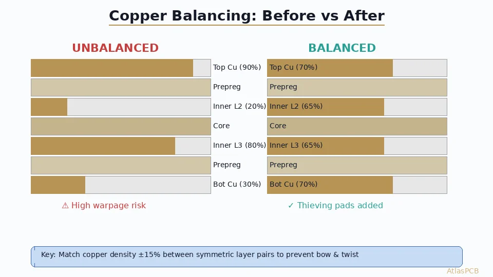
Cause 1: Asymmetric Copper Distribution
This is the single most common cause of PCB bow.
Copper has a coefficient of thermal expansion (CTE) of ~17 ppm/°C in-plane, while FR-4 epoxy/glass has ~14-16 ppm/°C. When one side of the board has significantly more copper than the other, the copper-heavy side constrains expansion more, causing the board to cup toward that side during cooling after lamination.
Critical metric: Compare total copper area (%) on the top half of the stackup vs. the bottom half. A difference greater than 15-20% often produces measurable bow.
Cause 2: Unbalanced Lamination Stackup
Even with symmetric copper, if the prepreg/core arrangement is not mirrored:
- Different resin content top vs. bottom creates CTE mismatch
- Mixed material types (e.g., high-Tg core on one side, standard on the other) warp during cooldown
- Unequal prepreg thickness creates different resin flow and residual stress
Cause 3: Lamination Press Conditions
The press cycle directly affects residual stress:
- Excessive heating rate (>5°C/min) creates thermal gradients through the board thickness
- Uneven platen temperature causes one side to cure before the other
- Insufficient pressure allows resin-starved areas with different mechanical properties
- Rapid cooldown locks in thermal stress that would otherwise relax at elevated temperature
Cause 4: Copper Plating Thickness Variation
Electroplated copper develops internal stress (typically compressive). If plating thickness varies significantly across the board or between sides:
- Heavier plating on one side creates bimetallic strip effect
- Pattern plating with very different densities top vs. bottom
- Panel plating followed by excessive etching on one side
Cause 5: Reflow Soldering Thermal Shock
Even a board that passes flatness inspection as-fabricated can warp during assembly:
- Peak reflow temperature exceeds Tg, allowing stress relaxation and reshaping
- Differential component mass (heavy heatsinks on one side) creates thermal mass asymmetry
- Multiple reflow cycles (double-sided SMT) accumulate deformation
Prevention Strategies in Design
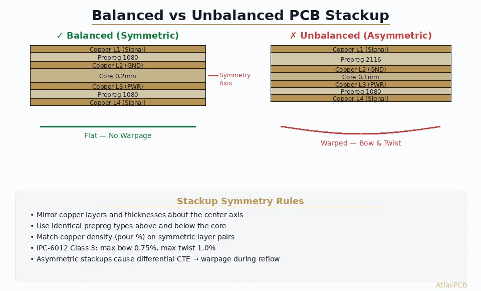
Strategy 1: Symmetric Stackup Design
The most effective prevention is designing a stackup where the top half mirrors the bottom half:
L1: Signal (35µm Cu)        ← Mirror axis
PP: 1080 × 1 (65% RC)      ↕
L2: GND Plane (35µm Cu)    ↕
Core: 0.2mm                 ↕ TOP HALF
L3: Signal (35µm Cu)        ↕
PP: 1080 × 1 (65% RC)      ↕
─── ─── ─── CENTER ─── ─── ───
PP: 1080 × 1 (65% RC)      ↕
L4: Signal (35µm Cu)        ↕ BOTTOM HALF
Core: 0.2mm                 ↕
L5: Power Plane (35µm Cu)  ↕
PP: 1080 × 1 (65% RC)      ↕
L6: Signal (35µm Cu)        ← Mirror axis
Rules:
- Same prepreg type and count above and below center
- Same core thickness and material grade
- Same copper weight on mirrored layers
- Same number of routing layers in each half
Strategy 2: Copper Balancing (Thieving)
When routing density differs between layers, add non-functional copper (thieving patterns) to equalize copper percentage:
- Target: ≥40% copper fill on every layer
- Use cross-hatched ground fill or dot patterns in open areas
- Match copper percentage within ±10% between mirrored layer pairs
- Apply copper thieving in the panel border (coupon area) as well as the board
Strategy 3: Panel Layout Optimization
Board position within the production panel affects warpage:
- Center the board array in the panel to ensure symmetric material flow during lamination
- Add copper balance borders around the board array
- Avoid mixing different board designs in one panel if they have vastly different copper densities
Strategy 4: Material Selection
Choose materials with matched CTE properties:
- Use the same prepreg type throughout the stackup
- For high-layer-count boards, consider low-CTE laminates (Megtron 6, IS415)
- Specify glass style that minimizes weave-induced CTE variation (spread glass 1078/2116)
Prevention in Fabrication
Controlled Press Profile
The lamination recipe is critical:
- Heating ramp: 2-3°C/min maximum (slower = more uniform temperature)
- Gel point hold: 15-20 minutes at resin flow temperature for uniform wetting
- Cure cycle: Full time at cure temperature (typically 180°C for standard FR-4)
- Cooldown: 2-3°C/min under pressure until below Tg
Post-Lamination Stress Relief
For boards that tend to warp or for critical applications:
- Bake panels at 150°C for 2-4 hours after lamination (before drilling)
- This allows residual stress to relax without deformation
- Particularly important for thick boards (>2.0 mm) and high-layer-count (>12 layers)
Storage and Handling
- Store panels vertically in racks (not stacked horizontally) to prevent creep
- Maintain temperature-controlled storage (18-25°C, <60% RH)
- Do not leave panels in direct sunlight or near heat sources
- Pre-bake panels before reflow if stored >24 hours at >60% RH
Measurement and Quality Control
Incoming Inspection
For critical assemblies, verify flatness on incoming bare boards:
- Sample size: Per IPC-6012, minimum 1 board per panel in each lot
- Measure both bow and twist independently
- Record values and trend over time to detect process drift
- Reject lots exceeding 0.75% (or your tighter specification)
In-Process Monitoring
Advanced fabricators measure flatness at multiple process steps:
- After lamination (before drilling) — baseline
- After pattern plating — detect plating-induced stress
- After solder mask — LPISM cure can add stress
- After HAL/ENIG — thermal processes can relieve or add stress
Statistical Process Control
Track flatness measurements using SPC methods:
- Cp/Cpk targets: >1.33 for the bow/twist measurement
- Control chart limits based on historical data
- Investigate any measurement outside ±2σ
- Annual capability study to validate process capability
Special Considerations for Advanced Applications
Large Board Assemblies (>300 mm)
Larger boards amplify the effects of bow and twist:
- The same 0.75% limit means more absolute deflection (e.g., 3 mm on a 400 mm diagonal)
- Tooling and fixtures must accommodate some deformation
- Consider panel routing (not scoring) to minimize edge stress
- Use vacuum fixtures for stencil printing to pull boards flat
Thin Boards (<0.8 mm)
Thin boards are inherently more flexible and prone to warpage:
- Lower stiffness means less force is needed to deform
- Must handle with vacuum tools during assembly
- Consider board stiffeners or carrier fixtures during reflow
- Specify tighter lamination controls (±0.05 mm thickness tolerance)
High-Tg and Halogen-Free Materials
Alternative laminate systems have different thermal behavior:
- High-Tg materials (Tg > 170°C) have different cure shrinkage characteristics
- Halogen-free resins often have higher CTE above Tg
- These materials may require modified press profiles
- Validate flatness separately when changing material systems
Further Reading
- PCB Stackup Symmetry and Balanced Lamination
- PCB Copper Balancing Techniques
- IPC-6012 ES Class Automotive and Aerospace PCBs
- What Causes PCB Delamination
Flatness You Can Count On
AtlasPCB operates controlled-atmosphere lamination presses with ±2°C platen uniformity and automated flatness inspection on every panel. Our standard process delivers ≤0.5% bow and twist on boards up to 24 layers — meeting automotive and aerospace requirements without special handling.
About AtlasPCB — We specialize in complex PCB manufacturing for HDI, RF, and high-reliability applications. Explore our multilayer PCB fabrication up to 30 layers, PCB assembly services, or get an full PCB manufacturing capabilities . Every order includes free engineering review. Get your quote.
Reviewed by AtlasPCB Engineering Team — IPC-certified manufacturing specialists with 15+ years of production experience in HDI, RF, and high-reliability PCB fabrication. Content based on factory floor data and real customer design reviews.
- pcb bow and twist
- IPC-TM-650
- warpage
- flatness
- lamination
- pcb manufacturing
- SMT assembly
- copper balancing
- stackup design