· AtlasPCB Engineering · Engineering · 11 min read
PCB Reflow Oven Profiling: Peak Temperature, Soak Time, and Defect Prevention for BGA Assembly
Master reflow soldering profile optimization for lead-free BGA assembly — covering preheat ramps, soak zone parameters, time above liquidus, peak temperature limits, and common reflow defects with prevention strategies.
Reflow soldering is the dominant assembly process for surface-mount technology, and getting the thermal profile right is the single most important factor in achieving consistent solder joint quality. For BGA packages — where hundreds or thousands of solder joints form simultaneously beneath the component body where visual inspection is impossible — profile optimization becomes critical.
This guide covers the engineering principles behind each zone of the reflow profile, practical parameter ranges for SAC305 lead-free solder, and defect mechanisms linked to profile deviations.
Anatomy of a Reflow Profile
A standard reflow profile consists of four distinct zones, each serving a specific metallurgical and chemical purpose. The profile is measured using thermocouples attached to the board at critical locations — typically the coldest point (usually the center of the largest ground plane), the hottest point (usually a small component near the board edge), and on BGA solder joints themselves.

Zone 1: Preheat (25°C → 150°C)
The preheat zone raises the board temperature from ambient to the flux activation range. The ramp rate must be carefully controlled:
- Target ramp rate: 1–3°C/s (recommended: 1.5–2.5°C/s)
- Duration: Typically 60–90 seconds
- Purpose: Gradually remove residual moisture, begin flux activation, prevent thermal shock
Why ramp rate matters: A ramp rate above 3°C/s creates thermal gradients within the board that can cause:
- Solder paste splattering as volatiles flash-evaporate
- Board warpage from uneven thermal expansion
- Component cracking in ceramic capacitors and BGAs
- Tombstoning of small passives (0201, 0402) due to differential pad heating
Conversely, a ramp rate below 1°C/s extends the total profile time unnecessarily, consuming flux before the critical reflow zone and reducing throughput.
Zone 2: Soak / Thermal Equalization (150–200°C, 60–120s)
The soak zone is arguably the most critical yet most frequently misunderstood portion of the reflow profile. Its purpose is threefold:
Flux activation — The flux chemistry in the solder paste begins actively reducing copper oxides on the pad surface and tin oxides on the solder particles. This chemical reaction requires both time and temperature.
Thermal equalization — Components on the board have vastly different thermal masses. A large BGA with a metal lid absorbs far more heat than an 0402 resistor. The soak zone allows temperatures across the board to converge, ensuring all joints reach the reflow zone within a narrow temperature window.
Volatile evacuation — Flux solvents and activator byproducts must evaporate during the soak zone. If they remain trapped in the paste when peak temperature is reached, they create voids within solder joints — particularly problematic for BGA packages where voids concentrate stress.
Process window guidelines:
| Parameter | Minimum | Recommended | Maximum |
|---|---|---|---|
| Temperature range | 150°C | 160–190°C | 200°C |
| Duration | 60s | 75–90s | 120s |
| ΔT across board | — | <10°C | 15°C |
| Ramp within soak | 0°C/s | 0.3–0.5°C/s | 1°C/s |
A common mistake is making the soak zone too hot (>200°C), which prematurely exhausts the flux activators before the critical reflow zone. The paste then has insufficient flux remaining to properly wet the pads at peak temperature.
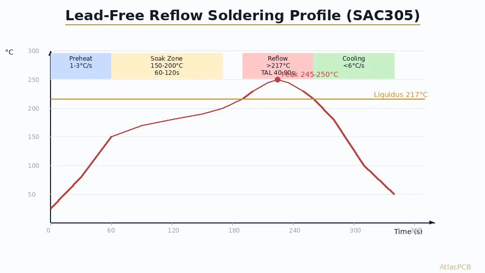
Zone 3: Reflow (>217°C, TAL 40–90s)
The reflow zone is where solder melts and metallurgical bonding occurs. Two parameters define this zone:
Peak Temperature: The highest temperature reached on the BGA solder joint.
- SAC305 liquidus: 217–220°C
- Minimum peak: 235°C (ensures all joints exceed liquidus even with ΔT)
- Recommended peak: 245–250°C
- Maximum peak: 260°C (MSL-3 limit per J-STD-020)
The peak temperature must exceed the liquidus by enough to ensure complete wetting and intermetallic compound (IMC) formation. For SAC305, the solder must be fully liquid for tin to diffuse into copper (or nickel for [ENIG-finished boards]/blog/enig-surface-finish-process/)) and form Cu₆Sn₅ or Ni₃Sn₄ intermetallic layers.
Time Above Liquidus (TAL): The duration during which the solder joint temperature exceeds 217°C.
- Minimum TAL: 30s (absolute minimum for IMC formation)
- Recommended TAL: 40–70s (optimal balance)
- Maximum TAL: 90s (excessive IMC growth beyond this point)
- For BGA packages: 60–90s preferred (solder balls under the package heat slower than exposed joints)
Insufficient TAL results in incomplete wetting and weak solder joints. Excessive TAL causes:
- Thick, brittle intermetallic layers (>3 μm) that reduce joint reliability
- Excessive copper dissolution into the solder, potentially consuming thin copper layers
- Component damage from prolonged high-temperature exposure
- Pad cratering in laminate substrates
Zone 4: Cooling (Peak → <100°C)
The cooling zone determines the microstructure of the solidified solder joint, which directly affects mechanical properties.
- Target cooling rate: 2–6°C/s
- Maximum cooling rate: 6°C/s (to prevent thermal shock)
- Minimum cooling rate: 1°C/s (to prevent excessive grain coarsening)
Fast cooling (4–6°C/s) produces fine-grained SAC solder microstructure with:
- Higher fatigue resistance
- Better tensile strength
- More uniform Ag₃Sn precipitate distribution
- Finer grain boundaries that impede crack propagation
Slow cooling (<2°C/s) produces coarse-grained microstructure with:
- Large Ag₃Sn platelets that act as crack initiation sites
- Lower fatigue life
- More susceptible to thermal cycling failures

Complex BGA Assembly? We Handle the Profile.
AtlasPCB provides complete PCB fabrication and assembly with optimized reflow profiles for every board — from 2-layer prototypes to 20+ layer HDI stacks.
Get Assembly QuoteCommon Reflow Defects and Profile-Related Root Causes
Head-in-Pillow (HiP)
HiP defects occur when the BGA solder ball and the solder paste on the pad both melt but fail to coalesce into a single joint. The result looks like a head resting on a pillow — two separate solder masses touching but not metallurgically bonded.
Profile-related causes:
- Board warpage during reflow causing the BGA ball to lift off the paste deposit
- Excessive oxidation of the ball surface due to too-long soak zone or exhausted flux
- ΔT too large — paste and ball reaching liquidus at different times
Profile fixes:
- Reduce soak zone time (keep flux active longer)
- Ensure ΔT < 10°C across the BGA footprint
- Use nitrogen atmosphere to reduce oxidation (O₂ < 500 ppm)
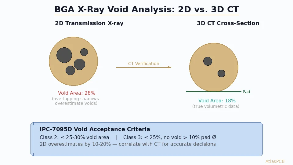
Solder Voiding
Voids in BGA solder joints concentrate mechanical stress and reduce thermal/electrical conductivity. IPC-7095 defines acceptable voiding levels: ≤25% void area for most applications, ≤10% for high-reliability.
Profile-related causes:
- Insufficient soak zone duration — volatiles trapped in paste
- Ramp rate too fast through 100–180°C range — explosive volatile release
- Excessive flux residue from too-low soak temperature
Profile fixes:
- Extend soak zone to 90–120 seconds
- Reduce preheat ramp to 1.5°C/s maximum
- Ensure soak zone reaches at least 160°C for complete volatile evacuation
Tombstoning
Tombstoning occurs when surface tension forces on one end of a chip component pull it into a vertical position during reflow.
Profile-related causes:
- Large thermal gradient across small components — one pad reaching liquidus before the other
- Excessive ramp rate during the transition from soak to reflow
Profile fixes:
- Improve board design by equalizing thermal mass around small components (see [DFM guidelines for fine-pitch design]/blog/dfm-fine-pitch-bga-pcb-design-rules/))
- Reduce ramp rate from soak to reflow zone
- Consider longer soak to equalize thermal mass
Cold Joints / Non-Wetting
Solder melts but fails to form a proper metallurgical bond with the pad.
Profile-related causes:
- Peak temperature too low (solder barely liquid, insufficient energy for IMC formation)
- TAL too short (<30 seconds)
- Flux exhausted during excessively long soak zone
Profile fixes:
- Increase peak temperature by 5–10°C (within component limits)
- Extend TAL to at least 40 seconds
- Shorten soak zone if flux exhaustion is suspected
Profiling Equipment and Methodology
Thermocouple Placement
Accurate profiling requires thermocouples at specific locations:
- BGA joint — attach K-type thermocouple (36 AWG) to a corner pad of the largest BGA using high-temperature solder or Kapton tape
- Board center — on the largest ground plane area (coldest point)
- Board edge — near a small component (hottest point)
- Connector area — if through-hole components will undergo wave or selective soldering later
The temperature difference between the hottest and coldest points (ΔT) is the primary metric for profile optimization. For BGA boards, ΔT should be:
- Standard: <15°C
- Fine-pitch BGA: <10°C
- High-reliability: <7°C
Oven Configuration
Modern reflow ovens provide 7–13 heating zones plus 1–3 cooling zones. General guidelines:
- Zones 1–3: Preheat — set progressively higher (150/160/170°C typical)
- Zones 4–6: Soak — set near the soak target (180/185/185°C typical)
- Zones 7–9: Reflow — ramp to peak (220/250/260°C typical)
- Zones 10+: Cooling — fans at maximum
- Conveyor speed: Adjust to hit the target profile duration (typically 4–6 minutes total)
Nitrogen atmosphere is recommended for lead-free BGA assembly:
- Reduces oxidation on solder and pad surfaces
- Improves wetting, especially on [OSP-finished boards]/blog/pcb-surface-finish-osp-enig-immersion-silver-lead-free-assembly/)
- Typical O₂ target: 500–1000 ppm (premium: <200 ppm)
Profile Optimization for Specific Board Characteristics
High Thermal Mass Boards
Boards with large copper pours, heavy ground planes, or embedded [thermal via arrays]/blog/pcb-thermal-via-design/) absorb significant heat. These boards require:
- Slower preheat ramp (1–1.5°C/s)
- Longer soak zone (100–120s)
- Potentially higher peak temperature (250–255°C) to ensure center-board joints reach proper reflow
Mixed-Technology Boards
Boards with both large BGA packages and small passives (0201/0402) create the widest ΔT challenges. Strategies:
- Use the longest soak zone the flux chemistry allows
- Consider ramp-soak-spike (RSS) profiles instead of tent profiles
- Place thermocouples on both the BGA and the smallest component to verify ΔT
Thick Boards (>2mm)
Thick, [high-layer-count boards]/blog/high-layer-count-pcb-challenges/) transfer heat slowly through their cross-section. Top-side and bottom-side temperatures may differ significantly. Solutions:
- Use bottom-side heating zones at slightly higher settings
- Extend total profile time by reducing conveyor speed
- Profile both top and bottom surfaces simultaneously
Nitrogen Atmosphere and Its Effect on Profile Optimization
The use of nitrogen (N₂) atmosphere in reflow ovens has become increasingly common for lead-free BGA assembly. Nitrogen reduces the partial pressure of oxygen at the solder joint, which has several profile-related benefits:
How Nitrogen Helps
Reduced oxidation: In air (21% O₂), solder paste oxidizes rapidly at temperatures above 150°C. This oxide formation consumes flux activators, meaning less flux is available for the critical wetting step at peak temperature. In nitrogen (O₂ < 1000 ppm), oxidation is dramatically slower, preserving flux for the reflow zone.
Wider process window: Because flux is consumed more slowly in nitrogen, the acceptable soak zone duration expands. A profile that might produce cold joints in air (due to flux exhaustion) can work perfectly in nitrogen. This wider window is particularly valuable for:
- Boards with high thermal mass variation (large ΔT)
- Mixed-technology assemblies requiring longer equalization time
- OSP-finished boards where the organic coating provides less protection than metallic finishes
Lower peak temperature option: Some manufacturers find they can reduce peak temperature by 5–10°C in nitrogen while maintaining equivalent wetting quality. This provides additional margin against component damage and board delamination.
Nitrogen Concentration Levels
Different O₂ concentration targets provide different levels of benefit:
- <1000 ppm O₂: Standard nitrogen reflow — noticeable improvement in wetting consistency
- <500 ppm O₂: Recommended for BGA assembly — significant reduction in voiding and HiP defects
- <200 ppm O₂: Premium nitrogen — best results for fine-pitch and high-reliability applications
- <100 ppm O₂: Ultra-high purity — used for flip chip and advanced packaging; diminishing returns for standard SMT
The cost of nitrogen depends on local supply and oven design. Tunnel ovens with effective nitrogen curtains at entry and exit consume 10–30 m³/hour. At typical industrial nitrogen prices, this adds $0.01–0.05 per board for medium-volume production — a small price for the quality improvement.
Profile Documentation and Quality Standards
IPC-7530 Guidelines
IPC-7530 (Guidelines for Temperature Profiling of Electronic Assemblies) establishes the framework for reflow profile development, including:
- Minimum and maximum thermocouple quantities per board size
- Thermocouple attachment methods and their measurement uncertainty
- Profile recording and storage requirements
- Statistical methods for determining process capability (Cpk)
For production environments, IPC-7530 recommends re-profiling whenever:
- A new board design enters production
- Oven maintenance or zone heater replacement occurs
- Solder paste formulation or lot changes
- Conveyor speed or oven recipe changes
- Environmental conditions change significantly (seasonal temperature shifts in non-climate-controlled facilities)
Profile as a Quality Record
In automotive (IATF 16949), aerospace (AS9100), and [medical device (ISO 13485)]/blog/medical-pcb-manufacturing-requirements/) manufacturing, reflow profiles are quality records that must be:
- Documented with thermocouple data files for each product
- Stored for the product retention period (often 15+ years for automotive)
- Available for customer audit upon request
- Traceable to the specific oven and recipe used for each production lot
Many advanced reflow ovens now include automatic profile logging that captures temperature data for every board processed, creating a continuous quality record without manual intervention.
Cost of Getting the Profile Wrong
The financial impact of profile-related defects is often underestimated:
- BGA rework: $5–50 per BGA depending on package size and board complexity. For a typical automotive ECU with 2 BGAs, rework costs easily exceed $100 per board.
- X-ray inspection: Adding 100% X-ray inspection for BGA solder joints costs $0.50–2.00 per board at volume. A well-optimized profile reduces the need for this expensive screening step.
- Field failures: A cold joint or HiP defect that escapes to the field can result in warranty costs 10–100× the manufacturing cost of the board. For automotive applications under IATF 16949, PPM (parts per million) defect targets demand near-zero profile-related failures.
- Scrap: Boards damaged by excessive reflow temperatures (delamination, pad cratering, component damage) are typically scrapped entirely. For complex multilayer boards costing $50–200 each, this is a significant loss.
Conclusion
Reflow profile optimization is an iterative process that balances competing requirements: sufficient heat for metallurgical bonding, minimal thermal exposure for component and board integrity, and controlled cooling for optimal microstructure. The parameters in this guide provide starting points, but every board design requires its own profiling exercise with thermocouple data.
The investment in proper profiling — typically 2–4 hours of engineering time per new design — pays for itself many times over through reduced defect rates, lower rework costs, and improved field reliability. For BGA assemblies in particular, where rework is expensive and X-ray inspection adds cost, getting the profile right the first time is the most cost-effective quality strategy available.
Outsourcing BGA assembly and want guaranteed profile optimization? AtlasPCB’s assembly team profiles every new design with thermal data logging and adjusts parameters until defect targets are met. Contact us for a quote on your next BGA assembly project.
Further Reading
- [BGA Pad Design and Via-in-Pad: Preventing Solder Voiding]/blog/bga-pad-design-via-in-pad-solder-voiding-prevention/)
- [BGA Rework and Reballing Process Guide]/blog/bga-rework-reballing-process-guide/)
- [AOI and SPI Inspection for PCB Assembly Quality Control]/blog/aoi-spi-inspection-pcb-assembly-quality-control/)
- [PCB Tombstoning: Root Causes and DFM Prevention Strategies]/blog/pcb-tombstoning-causes-prevention-dfm/)
About AtlasPCB — We specialize in complex PCB manufacturing for HDI, RF, and high-reliability applications. Explore our HDI PCB manufacturing capabilities, PCB assembly services, or get an aluminum and metal-core PCB services . Every order includes free engineering review. Get your quote.
Reviewed by AtlasPCB Engineering Team — IPC-certified manufacturing specialists with 15+ years of production experience in HDI, RF, and high-reliability PCB fabrication. Content based on factory floor data and real customer design reviews.
- reflow soldering
- BGA assembly
- solder profile
- lead-free
- SAC305
- PCB assembly
- thermal profiling
- soldering defects