· AtlasPCB Engineering · Engineering · 7 min read
PCB Laser Direct Imaging (LDI): Resolution Advantages Over Phototool Lithography for Fine-Pitch HDI Manufacturing
Compare PCB laser direct imaging (LDI) with conventional phototool lithography. Learn how LDI achieves 15μm line/space resolution without film registration errors, reduces DES defects, and enables cost-effective fine-pitch HDI and IC substrate manufacturing.
Introduction: The Lithography Bottleneck in PCB Manufacturing
Photolithography defines every copper feature on a printed circuit board — traces, pads, vias, and planes are all patterned through selective UV exposure of photoresist followed by chemical development. As PCB designs push toward finer features driven by HDI, IC substrate, and advanced packaging requirements, the imaging step becomes the resolution-limiting process in the fabrication sequence.
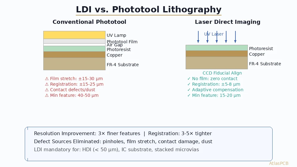
For decades, the industry relied on phototool lithography: creating a silver halide or diazo film from Gerber data, placing this film in direct contact with the resist-coated panel, and exposing through the film with a collimated UV source. This process works well for features above 50 μm but introduces systematic errors that limit further resolution improvement.
Laser Direct Imaging (LDI) bypasses the film entirely, using focused UV laser beams (typically 355 nm or 405 nm wavelength) to write patterns directly onto the photoresist. This digital-to-physical workflow eliminates an entire class of error sources and enables the fine-line patterning that modern electronics demand.
How Phototool Lithography Works — And Where It Fails
Conventional Process Flow
- Gerber-to-film conversion: Photo-plotter exposes silver halide master film from digital data
- Working film production: Contact-print copies from master for production use
- Film registration: Align film to panel using registration pins or optical alignment
- Contact exposure: Press film against resist-coated panel in vacuum frame; expose with mercury lamp (350–420 nm broadband)
- Development: Remove unexposed (negative process) or exposed (positive process) resist
Error Sources in Film-Based Imaging
Dimensional instability:
- Film substrate (PET base) has a coefficient of thermal expansion ~20 ppm/°C
- A 24” × 18” panel at +2°C temperature variation: ~25 μm dimensional shift
- Humidity absorption causes additional 10–15 ppm dimensional change
- Combined uncertainty: ±15–30 μm across panel area
Film degradation:
- Working films accumulate scratches, pinholes, and debris over 200–500 exposures
- Silver halide density decreases with UV exposure count (optical density drift)
- Edge sharpness degrades from handling damage
- Typical replacement frequency: every 200 exposures for Class 2, 100 for Class 3
Contact and vacuum artifacts:
- Newton’s rings from imperfect film-resist contact at local areas
- Trapped air bubbles create unexposed regions
- Dust particles between film and resist create pinholes (50–200 μm defects)
- Vacuum frame pressure variations cause focus depth inconsistency
Registration limitations:
- Pin registration: ±25 μm (mechanical tolerance of pin/hole system)
- Optical registration with CCD: ±15 μm (still limited by film dimensional drift)
- Front-to-back registration through panel: ±15–25 μm with manual flip
LDI Technology: Eliminating the Film
Operating Principles
LDI systems use one of three laser architectures:
Polygon mirror scanning (raster):
- Single high-power laser beam scanned across panel width by rotating polygon mirror
- Each scan line: 1–10 μm pixel pitch depending on lens and polygon facets
- Throughput: 20–60 panels/hour for 24” × 18” format
- Examples: Orbotech Nuvogo, MIVA Direct Imaging
DMD (Digital Micromirror Device) projection:
- Array of 1–4 million individually addressable mirrors (Texas Instruments DLP chip)
- Each mirror directs UV light toward or away from panel surface
- Massive parallelism: expose thousands of pixels simultaneously
- Higher throughput: 60–120 panels/hour
- Examples: Screen GP series, Dainippon Screen
Laser diode array:
- Multiple independently modulated laser diodes in a linear array
- Combine scanning and parallel exposure
- Balance throughput and resolution
- Examples: Limata, Mycronic
Resolution Capability
LDI achieves its resolution advantage through:
- No contact gap: Laser focuses directly on resist surface (working distance 5–50 mm, autofocus maintains ±1 μm depth)
- Pixel-based patterning: Each exposure point is individually controlled; no mask edge diffraction
- Thermal compensation: Panel temperature and humidity measured in real-time; exposure pattern scaled to match actual panel dimensions
- Adaptive alignment: Fiducials scanned before exposure; panel distortion mapped and compensated in software
Production resolution by technology:
- Polygon LDI: 15–20 μm line/space (standard), 10–15 μm (high-performance)
- DMD projection: 20–30 μm (standard throughput mode), 15 μm (high-resolution mode)
- Advanced LDI for IC substrates: 8–12 μm line/space
Direct Comparison: LDI vs. Phototool
Resolution and Accuracy
| Parameter | Phototool | LDI |
|---|---|---|
| Minimum line/space | 40–50 μm production | 15–20 μm production |
| Registration accuracy | ±15–25 μm | ±5–8 μm |
| Dimensional stability | ±15–30 μm (temp/humidity) | ±3–5 μm (digital compensation) |
| Repeatability | Degrades with film age | Constant (digital data) |
| Pad-to-hole registration | ±25 μm | ±8–12 μm |
Defect Comparison
| Defect Type | Phototool Cause | LDI Status |
|---|---|---|
| Pinholes (resist) | Dust on film | Eliminated (no contact) |
| Open circuits | Film scratches | Eliminated |
| Shorts | Over-exposure from density loss | Eliminated |
| Pattern shift | Film stretch | Compensated digitally |
| Registration error | Mechanical alignment | Reduced by 3–5× |
| Focus variation | Contact pressure uneven | Autofocus per point |
Economic Comparison
Phototool costs (per month, 500 unique layers):
- Film procurement: $50K–$150K (film + development chemistry)
- Film handling labor: $15K–$30K (inspection, mounting, cleaning, storage)
- Yield loss from film defects: 0.5–2% additional scrap
- Film storage: Climate-controlled room required
LDI costs (per month):
- Equipment depreciation: $8K–$15K/month (based on $1M system, 7-year life)
- Laser source replacement: $5K–$10K/year
- No film, no storage, no film-related yield loss
- Software license: $5K–$10K/year
Throughput Considerations
Standard phototool exposure: 40–80 panels/hour (quick exposure, slow setup) Production LDI: 30–120 panels/hour depending on resolution mode and technology
The throughput gap has narrowed dramatically. Modern DMD-based LDI systems match or exceed phototool throughput for panels with 3+ imaging layers, since LDI eliminates film changeover time between designs.
Need Fine-Line HDI PCBs with Tight Registration?
AtlasPCB uses LDI for all HDI and fine-pitch designs. Our process achieves 25 μm line/space with ±8 μm layer-to-layer registration for your demanding designs.
Get a Quote →When LDI Is Mandatory vs. Optional
LDI Mandatory (Cannot Achieve with Film)
- HDI designs with 25–40 μm line/space
- Stacked microvias requiring 20–25 μm annular ring (registration budget demands ±8 μm)
- IC substrate fabrication (< 20 μm features)
- Designs where front-to-back registration must be < ±10 μm
- Mixed-material panels with significant dimensional variation (rigid-flex transitions)
- UHDI (Ultra HDI) with via-in-trace features
LDI Recommended (Significant Quality Improvement)
- Standard HDI with 50–75 μm features (yield improvement from eliminating film defects)
- High-mix production (> 100 designs/month where film management becomes complex)
- Medical and aerospace PCBs requiring zero-defect imaging certification
- Panels with large area variation (temperature-sensitive materials like PTFE)
Conventional Film Still Suitable
- Standard multilayer with features > 100 μm
- High-volume, single-design production runs (> 10,000 panels of same design)
- Basic 2-layer PCBs with relaxed tolerances
- Very thick panels (> 3 mm) where feature size is proportionally large
Process Integration: LDI in the Full Fabrication Flow
Resist Selection for LDI
LDI systems use different photoresist chemistries than broad-spectrum lamp exposure:
- Wavelength sensitivity: LDI resists optimized for 355 nm (tripled Nd:YAG) or 405 nm (GaN diode) laser
- Photospeed: Higher sensitivity required due to lower per-pixel dose (compensated by slower write speed or higher power)
- Contrast: Higher contrast (gamma > 3.0) enables sharper edges with single-pass exposure
- Thickness: Typically 15–40 μm dry film; thinner films (8–12 μm) for finest features
Common LDI-optimized resists: Hitachi RY-5000 series, Asahi Kasei Sunfort, DuPont Riston LDI series
Data Preparation
LDI eliminates film but requires optimized data handling:
- Gerber/ODB++ import with scaling compensation pre-applied
- Rasterization at LDI native resolution (typically 0.5–2 μm pixel grid)
- Panel layout optimization for write time minimization
- Compensation features for resist development effects (undercut prediction)
- Fiducial placement for real-time alignment during exposure
Quality Control
LDI enables unique quality verification:
- Post-exposure imaging: Some systems capture reflectance image after exposure for immediate defect detection
- Dose mapping: Record actual delivered energy per pixel for process traceability
- Alignment verification: Report actual panel distortion correction applied
- SPC integration: Automated tracking of focus quality, power stability, and registration accuracy
Industry Trends: LDI Market Growth
The LDI market in PCB manufacturing has grown approximately 15% annually from 2020 to 2026, driven by:
- 5G infrastructure: Base station PCBs require 30–50 μm features with tight impedance control
- AI/ML hardware: High-layer-count PCBs for GPU/ASIC packages need consistent layer registration
- Automotive ADAS: Safety-critical designs mandate imaging process traceability
- Packaging substrates: Organic IC substrates approaching semiconductor-like features (5–15 μm)
- Miniaturization: Consumer devices driving HDI adoption in mid-range products
Further Reading
- [HDI Microvia: Stacked vs. Staggered Reliability]/blog/hdi-microvia-stacked-vs-staggered-reliability/) — Via structures enabled by LDI precision
- [PCB Copper Plating Uniformity and Throwing Power]/blog/pcb-copper-plating-uniformity-throwing-power-pattern-plating/) — The plating process that follows LDI patterning
- [Controlled Impedance PCB Design and Stackup]/blog/controlled-impedance-pcb-design-stackup-calculations/) — How LDI registration affects impedance tolerance
- [PCB Solder Mask Application: LPI vs. Dry Film vs. Inkjet]/blog/pcb-solder-mask-application-lpi-vs-dry-film-inkjet/) — Complementary imaging for solder mask layers
Conclusion
Laser Direct Imaging has transitioned from a premium option to a mainstream requirement for modern PCB manufacturing. The elimination of phototool film removes an entire category of defect sources, improves registration by 3–5×, and enables feature sizes that are physically impossible with contact lithography. For any design with features below 50 μm or registration requirements below ±15 μm, specify an LDI-capable fabricator to ensure consistent yield and reliability.
Designing HDI or fine-pitch PCBs? Request an engineering review from AtlasPCB to validate your design against our LDI process capabilities.
About AtlasPCB — We specialize in complex PCB manufacturing for HDI, RF, and high-reliability applications. Explore our HDI PCB manufacturing capabilities, or get an full PCB manufacturing capabilities . Every order includes free engineering review. Get your quote.
Reviewed by AtlasPCB Engineering Team — IPC-certified manufacturing specialists with 15+ years of production experience in HDI, RF, and high-reliability PCB fabrication. Content based on factory floor data and real customer design reviews.
- LDI
- laser direct imaging
- PCB manufacturing
- phototool
- lithography
- HDI
- fine-line
- DES
- photoresist
- IC substrate