· AtlasPCB Engineering · Engineering · 8 min read
Grounded Coplanar Waveguide (GCPW) PCB Design: When to Choose CPW Over Microstrip for RF Routing
Complete guide to grounded coplanar waveguide (GCPW) design on PCB, covering impedance calculation, gap geometry, via stitching requirements, and comparison with microstrip for mmWave, 5G, and high-frequency applications above 10 GHz.
Introduction: Why Microstrip Isn’t Enough Above 10 GHz
Microstrip has served as the default PCB transmission line topology for decades. Its single-layer routing simplicity and well-understood design rules make it the natural first choice for RF interconnects from DC through X-band (8–12 GHz).
But as operating frequencies push into K-band, Ka-band, and millimeter-wave territory — driven by 5G NR (FR2), automotive radar (77 GHz), and satellite communications (Ka-band, 26–40 GHz) — microstrip’s limitations become increasingly problematic:
- Radiation loss increases with frequency squared — at 28 GHz, microstrip loses 0.5–1.0 dB/cm from radiation alone
- Surface wave excitation — substrate modes couple power away from the intended signal path
- Dispersion — effective dielectric constant becomes frequency-dependent, distorting wideband signals
- Poor isolation — adjacent microstrip traces couple through fringing fields over large distances
Grounded Coplanar Waveguide (GCPW) addresses all four problems through its shielded geometry. The coplanar ground strips confine electric fields to the gap region, dramatically reducing radiation and coupling. The via-stitched ground cage suppresses substrate modes entirely.
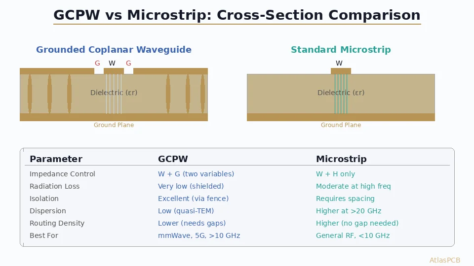
GCPW Geometry and Physics
A GCPW cross-section consists of five elements:
- Signal trace — center conductor with width W
- Coplanar gaps — slot regions of width G on each side of the signal trace
- Coplanar ground strips — wide ground conductors flanking the gaps (same metal layer)
- Dielectric substrate — the PCB laminate with height H and permittivity εr
- Bottom ground plane — continuous reference plane on the next copper layer
The electromagnetic mode in GCPW is quasi-TEM — similar to microstrip but with electric field lines concentrated in the narrow gap regions rather than spreading into free space above the trace. This confinement is the source of GCPW’s superior performance at high frequencies.
Field Distribution
In microstrip, roughly 50% of the electric field propagates through air above the trace. This air-dielectric interface causes frequency-dependent effective permittivity (dispersion).
In GCPW, approximately 70–80% of the field is concentrated in the gap regions within the substrate. The reduced air interaction means:
- Lower dispersion (more consistent group delay)
- Less radiation (fields are contained)
- Better shielding (coplanar grounds absorb stray fields)
Impedance Design: The W-G-H Triangle
GCPW impedance is controlled by three geometric parameters:
- W (trace width): Wider → lower impedance
- G (gap width): Wider gaps → higher impedance
- H (substrate height): Thicker substrate → higher impedance (microstrip-like contribution)
The dual-control mechanism (both W and G affect Z₀) gives GCPW designers more flexibility than microstrip, where only W and H are available. This is particularly valuable when:
- The substrate height is fixed by stackup constraints
- You need 50Ω on a thin dielectric where microstrip trace would be impractically narrow
- You need different impedances on the same layer without changing stackup
Typical 50Ω GCPW Dimensions
| Substrate | εr | H (mm) | W (mm) | G (mm) |
|---|---|---|---|---|
| Rogers RO4003C | 3.38 | 0.203 | 0.30 | 0.15 |
| Rogers RO4350B | 3.48 | 0.254 | 0.35 | 0.18 |
| Isola I-Tera MT40 | 3.45 | 0.100 | 0.15 | 0.10 |
| Megtron 6 | 3.4 | 0.127 | 0.18 | 0.12 |
Note: These are starting-point values. Final dimensions MUST be validated with a 2.5D field solver accounting for copper roughness, solder mask loading, and via effects.
Via Stitching: The Critical Detail
The via fence connecting coplanar ground to the bottom ground plane is not optional decoration — it is structurally required for GCPW to function correctly. Without adequate via stitching, the parallel-plate waveguide formed between the top coplanar ground and bottom ground plane supports resonant modes that:
- Create unexpected notches in the transmission response (S21 nulls)
- Radiate at resonant frequencies
- Couple into adjacent transmission lines through the substrate
Via Spacing Rule
The fundamental rule: via-to-via pitch ≤ λ/20 at the highest operating frequency.
| Frequency | λ₀ (free space) | λ in substrate (εr≈3.4) | λ/20 pitch |
|---|---|---|---|
| 6 GHz | 50 mm | 27 mm | 1.35 mm |
| 15 GHz | 20 mm | 10.8 mm | 0.54 mm |
| 28 GHz | 10.7 mm | 5.8 mm | 0.29 mm |
| 60 GHz | 5 mm | 2.7 mm | 0.135 mm |
| 77 GHz | 3.9 mm | 2.1 mm | 0.106 mm |
At 77 GHz, the required via pitch (0.1 mm) approaches the limit of standard PCB drilling technology. This is where laser-drilled microvias and HDI stackup techniques become essential for mmWave GCPW design.
Via Diameter and Pad Size
For RF via stitching:
- Via drill: 0.15–0.25 mm (smaller = less parasitic capacitance)
- Via pad: drill + 0.15 mm annular ring minimum
- Anti-pad in signal layers: standard clearance (0.2 mm gap from via pad)
RF & mmWave PCB Fabrication
AtlasPCB manufactures GCPW structures with ±10% impedance tolerance on Rogers, Isola, and Taconic RF laminates. Laser-drilled via stitching down to 0.1 mm pitch.
Get RF PCB Quote →GCPW vs Microstrip: Decision Framework
Choose GCPW When:
- Operating above 10–15 GHz — radiation loss and dispersion in microstrip become significant
- Adjacent trace isolation is critical — GCPW provides 15–20 dB better isolation than equivalent microstrip spacing
- Wideband performance required — lower dispersion means flatter group delay across multi-octave bandwidth
- Chip-to-board transitions — many MMIC/RFIC packages use CPW pad geometry; GCPW provides impedance-matched launch
- EMI compliance — shielded GCPW radiates 10–20 dB less than microstrip at equivalent frequency
Choose Microstrip When:
- Frequency below 6 GHz — microstrip is adequate and simpler to route
- Routing density is the priority — GCPW consumes 3–4× more board space (signal + two gaps + ground strips)
- Thick substrates — at H > 0.5 mm, microstrip actually performs well because fields are better confined
- Cost sensitivity — microstrip requires no via stitching, saving drill count and manufacturing complexity
- Mixed-signal boards — digital + low-frequency RF sections route more efficiently as microstrip
Hybrid Approach
Many practical designs use both topologies:
- GCPW for antenna feeds, LNA inputs, and mmWave interconnects
- Microstrip for IF stages, bias lines, and lower-frequency RF paths
- Transitions between the two use tapered structures (graded ground gap)
Transitions and Discontinuities
GCPW-to-Microstrip Transition
When transitioning from GCPW to microstrip (e.g., moving from an RF connector footprint to internal routing), the coplanar ground must terminate gradually:
- Taper the gap width from G to ∞ over a length of λ/4
- End the coplanar ground strips with the last via stitch
- Allow the trace width to adjust for impedance continuity (microstrip width differs from GCPW width for the same Z₀)
A well-designed transition adds < 0.1 dB insertion loss and maintains VSWR < 1.3:1 through 40 GHz.
GCPW Bends and Corners
Right-angle bends in GCPW create impedance discontinuities and mode conversion. Mitigation techniques:
- Mitered corners — chamfer the outer corner at 45° to reduce excess capacitance
- Curved bends — radius ≥ 3× trace width eliminates sharp discontinuities
- Compensated bends — reduce trace width at the apex to counteract the capacitive loading
The coplanar ground strips must follow the bend continuously — any gap in the ground strip creates a radiating slot.
Practical Design Tips
1. Ground Strip Width
The coplanar ground strip on each side should be ≥ 3× the gap width (ideally ≥ 5×). Narrow ground strips don’t provide adequate field confinement and the transmission line behaves as lossy CPW rather than true GCPW.
2. Solder Mask Considerations
Solder mask over GCPW traces changes the effective permittivity by 2–5%, shifting impedance. For precision applications (±5% impedance tolerance), either:
- Remove solder mask from all GCPW regions (mask relief)
- Account for mask loading in simulation (εr,mask ≈ 3.5–4.0, thickness 15–25 μm)
3. Surface Roughness Impact
Copper roughness dominates GCPW loss above 30 GHz. At 77 GHz, switching from standard foil (Rz = 5 μm) to HVP foil (Rz = 1.5 μm) reduces insertion loss by 0.3–0.5 dB/cm. Always specify VLP or HVLP copper for GCPW designs above 20 GHz.
4. Stack-up Optimization
For GCPW-dominant designs, optimize the stackup for RF performance:
- Thin core under GCPW layer (0.1–0.2 mm) — this is H in the impedance calculation
- Low-loss laminate for the GCPW dielectric layer (Df < 0.004 at target frequency)
- Standard FR-4 acceptable for non-RF layers (power, digital) to manage cost
This hybrid stackup approach keeps material costs reasonable while delivering excellent RF performance. See our guide on high-speed material Dk/Df comparison for laminate selection.
Simulation and Verification
Pre-Layout Simulation
Before committing to a stackup, simulate the GCPW cross-section with a 2D field solver (Polar Si9000, Simbeor, or ATLC). Key outputs:
- Characteristic impedance (Z₀) vs. frequency
- Effective dielectric constant (εeff) vs. frequency
- Conductor loss (αc) and dielectric loss (αd) per unit length
- Coupling to adjacent GCPW traces vs. separation
Post-Layout Verification
After routing, extract the 3D structure and simulate with HFSS, CST, or EMPro:
- S-parameter of critical interconnects (S21 insertion loss, S11 return loss)
- Via transition performance (ensure no resonances below maximum frequency)
- Far-field radiation pattern (verify shielding effectiveness)
TDR Measurement
Time-Domain Reflectometry validates the fabricated GCPW impedance. The TDR response should show:
- Flat 50Ω plateau along GCPW sections
- Smooth transitions at GCPW-to-microstrip junctions
- No resonant ripples (which indicate via spacing issues)
AtlasPCB provides impedance testing with TDR verification on all controlled-impedance RF boards.
Conclusion
GCPW is the workhorse transmission line for modern RF/mmWave PCB design. Its field confinement, isolation performance, and dispersion control make it indispensable above 10 GHz. The trade-off is routing density and manufacturing complexity (via stitching requirements) — but for designs where signal integrity at high frequencies is non-negotiable, GCPW delivers measurably superior results.
As 5G mmWave, automotive radar, and satellite communications continue pushing operating frequencies higher, GCPW expertise becomes a competitive differentiator for both designers and manufacturers.
Designing RF/mmWave boards? AtlasPCB specializes in controlled-impedance GCPW fabrication with ±10% tolerance, laser-drilled via stitching, and TDR verification. Get a quote →
Further Reading:
About AtlasPCB — We specialize in complex PCB manufacturing for HDI, RF, and high-reliability applications. Explore our RF and high-frequency PCB services, or get an impedance-controlled PCB manufacturing . Every order includes free engineering review. Get your quote.
Reviewed by AtlasPCB Engineering Team — IPC-certified manufacturing specialists with 15+ years of production experience in HDI, RF, and high-reliability PCB fabrication. Content based on factory floor data and real customer design reviews.
- GCPW
- coplanar waveguide
- RF PCB design
- microstrip
- mmWave
- 5G
- transmission line
- impedance