· AtlasPCB Engineering · Engineering · 17 min read
Multilayer PCB Warpage Simulation: FEA Methods, IPC Standards & Design Control
Learn how to predict and control PCB warpage using FEA simulation. Covers IPC bow/twist specs, copper balancing, and process optimization for multilayer boards.

Why Warpage Matters in Multilayer PCBs
Warpage is one of the most persistent challenges in [multilayer PCB manufacturing]/blog/multilayer-fr4-pcb-manufacturer/). As a board curves, bows, or twists away from its intended flat profile, every downstream process suffers — from solder paste deposition and component placement to reflow soldering and final assembly yield. A board that measures 0.3 mm of bow across a 200 mm diagonal may seem minor, but for BGA packages with sub-0.5 mm pitch, that deformation can mean the difference between reliable joints and wholesale defects.
The problem intensifies with modern design trends. Thinner boards, higher layer counts, asymmetric copper distributions, and mixed-material stackups all increase the risk of warpage. As products push toward 20+ layer designs at thicknesses below 2.0 mm, the industry can no longer rely on trial-and-error. Engineers need predictive tools — and that is where finite element analysis (FEA) simulation enters the picture.
This article provides a comprehensive guide to understanding, simulating, and controlling warpage in multilayer PCBs. We cover the root causes, walk through FEA modeling methodologies, review IPC standards for [bow and twist]/blog/pcb-bow-and-twist-specification/), and detail practical design and manufacturing strategies for warpage mitigation.
Root Causes of PCB Warpage
Before modeling warpage, engineers must understand the physical mechanisms that drive it. PCB warpage arises from internal stress imbalances that develop during thermal processing — primarily lamination and reflow soldering.
CTE Mismatch Between Materials
The coefficient of thermal expansion (CTE) is the fundamental driver. Copper has a CTE of approximately 17 ppm/°C, while FR-4 epoxy resin expands at roughly 14–18 ppm/°C in the X-Y plane and 60–70 ppm/°C in the Z-axis below Tg. When the board heats during lamination (typically 180–200°C) and then cools, the differential contraction between copper layers and dielectric layers generates internal stresses.
The key insight is that it is not the absolute CTE values that cause warpage — it is the asymmetry of those values across the board’s cross-section. A perfectly symmetric stackup with identical copper densities on mirrored layers will develop balanced stresses that cancel out, producing a flat board. Any deviation from symmetry creates a net bending moment.
Asymmetric Copper Distribution
In practice, signal routing rarely produces identical copper coverage on mirrored layers. A 12-layer board might have 85% copper on Layer 2 (a ground plane) but only 40% copper on Layer 11 (a signal layer). This imbalance means the side with more copper contracts less during cooling, while the side with less copper (more resin) contracts more — causing the board to bow toward the copper-heavy side.
[Copper balancing techniques]/blog/pcb-copper-balancing-techniques/) are among the most effective tools for warpage control. The goal is to equalize copper density on each pair of mirrored layers (L1/Ln, L2/Ln-1, etc.) to within 10% or better.
Resin Flow and Content Imbalance
During lamination, prepreg resin melts and flows to fill gaps around copper features. Layers with low copper density absorb more resin, while dense copper planes leave less void space. If the resin content is not balanced across the stackup, the resulting dielectric thicknesses vary — and with them, the mechanical properties. Uneven resin distribution also means uneven shrinkage during cure, contributing to residual stress.
Lamination Process Effects
The lamination thermal profile itself affects warpage. Non-uniform heating across the press, uneven pressure distribution, and cooling rate asymmetries all create localized stress gradients. Rapid cooling locks in thermal stresses that might have relaxed under slower, more controlled profiles.
Board Geometry and Aspect Ratio
Warpage magnitude is strongly influenced by geometry. Thin boards warp more than thick ones for the same internal stress. Boards with high length-to-width aspect ratios tend to develop bow (curvature along one axis), while square boards may exhibit twist (opposite corners lifting). Panel size, routing pattern, and the location of the board within the production panel also play roles.
FEA Simulation Methodology for Warpage Prediction
Finite element analysis allows engineers to model the thermo-mechanical behavior of a multilayer PCB stackup and predict warpage before committing to fabrication. This section outlines the simulation workflow used by leading PCB design teams.
Step 1: Geometry and Stackup Definition
The simulation begins with a detailed representation of the [PCB stackup]/blog/multilayer-pcb-stackup-design-guide/). Each layer — copper, prepreg, and core — is modeled as a separate element set with its own thickness and material properties. The geometry is typically a 2D shell model extruded to 3D, or a full 3D solid model for complex cases.
Key inputs include:
- Layer count and sequence — the exact order of copper, prepreg, and core layers
- Copper thickness per layer — typically 17.5 µm (½ oz), 35 µm (1 oz), or 70 µm (2 oz)
- Dielectric thickness — prepreg and core thicknesses after lamination
- Copper pattern density per layer — percentage of copper remaining after etching, ideally extracted from Gerber data
- Board outline dimensions — including any cutouts, slots, or panel features
Step 2: Material Property Assignment
Accurate material characterization is critical for simulation fidelity. Each material requires the following thermo-mechanical properties:
Copper foil:
- Young’s modulus: ~117 GPa
- Poisson’s ratio: 0.34
- CTE: 17 ppm/°C
- Yield strength: 200–300 MPa (depending on foil type)
FR-4 prepreg/core (typical woven glass/epoxy):
- In-plane modulus (Ex, Ey): 18–24 GPa
- Out-of-plane modulus (Ez): 8–10 GPa
- In-plane CTE: 14–18 ppm/°C
- Z-axis CTE: 50–70 ppm/°C (below Tg), 250–300 ppm/°C (above Tg)
- Glass transition temperature (Tg): 130–180°C depending on resin system
The FR-4 material exhibits orthotropic behavior — its properties differ along the warp (machine direction), fill (cross direction), and Z-axis due to the woven glass reinforcement. Accurate simulation must account for this anisotropy rather than treating the laminate as isotropic.
For layers with patterned copper, the simulation uses effective (homogenized) properties that blend copper and dielectric based on the copper area fraction:
E_effective = E_copper × copper_fraction + E_dielectric × (1 − copper_fraction)
Similar mixing rules apply for CTE, though the Schapery or Turner models provide better accuracy for composite CTE estimation than simple rule-of-mixtures.
Step 3: Meshing Strategy
The model is discretized into finite elements. For PCB warpage simulation:
- Shell elements (e.g., SHELL181 in commercial FEA packages) are efficient for thin structures and provide good accuracy when the board thickness is much smaller than its planar dimensions
- Solid elements (e.g., SOLID186) offer higher fidelity for thick boards or when through-thickness stress distribution is important
- Element size should be fine enough to capture copper pattern variations — typically 0.5–2.0 mm in-plane, with at least one element through each physical layer thickness
For a 300 mm × 250 mm, 12-layer board, a typical model contains 50,000–200,000 elements depending on mesh density and whether solid or shell elements are used.
Step 4: Thermal Loading and Boundary Conditions
The simulation applies a thermal load that mimics the lamination cooling cycle:
- Initial temperature: Set to the peak lamination temperature (typically 180–200°C), representing the stress-free state where the resin cures and bonds all layers
- Final temperature: Room temperature (25°C)
- Temperature change (ΔT): The difference drives thermal contraction and stress development
Boundary conditions prevent rigid-body motion while allowing free deformation:
- A single node is fixed in X, Y, and Z (pinned)
- A second node is constrained in Y and Z (roller along X)
- A third node is constrained in Z only (planar constraint)
This “3-2-1” constraint scheme eliminates the six rigid-body degrees of freedom without introducing artificial reaction forces that would distort the warpage prediction.
Step 5: Solving and Post-Processing
The solver computes the displacement field under the thermal load. The key output is the Z-displacement contour across the board surface, which directly represents warpage. From this field, engineers extract:
- Maximum bow: The largest single-axis curvature, calculated as the maximum Z-deviation along the longest diagonal divided by the diagonal length, expressed as a percentage
- Maximum twist: The deviation from planarity at the four corners, divided by the diagonal length
- Warpage direction: Concave (smiling) vs. convex (frowning) — important for assembly process planning
Modern FEA tools can also model the reflow soldering cycle, where a second thermal excursion to 245–260°C temporarily softens the FR-4 resin, allowing partial stress relaxation before re-cooling introduces new stresses. This two-step analysis provides a more realistic prediction of the board’s warpage state at the point of component attachment.
Simulation Accuracy and Validation
Well-calibrated FEA models can predict warpage within 10–15% of measured values. The main sources of error include:
- Inaccurate material property data (particularly temperature-dependent CTE curves)
- Simplified copper pattern representation (area fraction vs. actual pattern geometry)
- Neglecting viscoelastic relaxation in the resin during slow cooling
- Ignoring moisture absorption effects (FR-4 absorbs 0.1–0.3% moisture, which affects CTE)
Correlation studies between simulation and physical measurement are essential for calibrating model parameters. Once calibrated against a few test builds, the model becomes a reliable predictive tool for future designs.
IPC Standards for Bow and Twist
The IPC (Association Connecting Electronics Industries) defines the test methods and acceptance criteria for PCB warpage through several interrelated specifications.
IPC-TM-650, Method 2.4.22
This is the standard test method for measuring [bow and twist]/blog/pcb-bow-and-twist-specification/) in printed boards. It defines:
- Bow: A cylindrical or spherical curvature of the board such that all four corners remain in contact with a flat surface, with the center region elevated (or depressed)
- Twist: A deformation where one corner lifts off the flat surface while the diagonally opposite corner remains in contact — a helical or propeller-like distortion
The measurement is performed by placing the board on a flat reference surface and measuring the maximum deviation using a height gauge, feeler gauge, or optical measurement system. The result is expressed as a percentage:
Warpage (%) = (Maximum Deviation / Diagonal Length) × 100
IPC-6012 Acceptance Criteria
IPC-6012 (Qualification and Performance Specification for Rigid Printed Boards) specifies the following limits:
| Board Type | Maximum Bow & Twist |
|---|---|
| Surface mount components | ≤ 0.75% |
| Through-hole only | ≤ 1.5% |
| BGA/fine-pitch (industry practice) | ≤ 0.5% |
For boards destined for BGA assembly, the 0.75% IPC limit is often insufficient. Many EMS providers specify ≤ 0.5% or even ≤ 0.3% for large BGA packages (≥ 35 mm body size) where coplanarity is critical. When designing [high-layer-count boards]/blog/high-layer-count-pcb-challenges/) for advanced assemblies, these tighter tolerances should be the design target from the outset.
IPC-A-600 Visual Acceptance
IPC-A-600 provides visual acceptance criteria and includes bow and twist evaluation as part of incoming inspection for bare boards. It references the measurement methodology of TM-650 2.4.22 and the limits of IPC-6012.
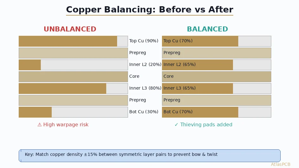
Copper Balancing Strategies for Warpage Control
Copper balancing is the single most impactful design strategy for minimizing warpage. The principle is straightforward: ensure that mirrored layer pairs have matched copper densities so that thermal contraction is symmetric about the board’s neutral axis.
Layer-Pair Matching
For an N-layer board, the critical pairs are:
- Layer 1 and Layer N
- Layer 2 and Layer N−1
- Layer 3 and Layer N−2
- And so on toward the center
Each pair should have copper coverage within 10% of each other. For example, if Layer 3 is a ground plane at 82% copper, then Layer N−2 should also have at least 72% copper coverage.
Adding Copper Fill (Thieving)
When functional routing cannot achieve balanced copper, engineers add non-functional copper fill — commonly called copper thieving or copper balancing patterns. These are electrically isolated pads, hatched fills, or solid pours added to low-density layers to increase their overall copper percentage.
Best practices for copper thieving:
- Use a regular grid of small pads (0.5–1.0 mm diameter, 1.0–2.0 mm pitch) rather than solid fills, to maintain consistent etching and avoid trapped acid
- Keep thieving patterns away from impedance-controlled traces where they might affect characteristic impedance
- Apply thieving uniformly across the entire layer, not just in localized areas — localized fill can create its own stress concentrations
- Coordinate thieving with the fabricator, as they may have preferred patterns for their process
Copper Density Analysis Tools
Modern PCB CAD systems include copper density analysis tools that display a color-coded heat map of copper coverage per layer. Designers should review these maps for every layer pair and iterate until the balance is within tolerance. Some advanced tools can automatically suggest thieving patterns to achieve a target balance.
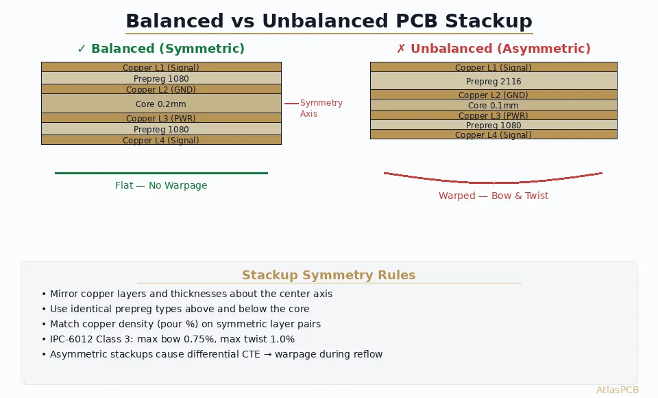
Stackup Symmetry Design
Beyond copper balancing, the physical [stackup design]/blog/pcb-stackup-design-guide/) must be symmetric about the board’s center plane.
Structural Symmetry
A symmetric stackup means that the material types and thicknesses are mirrored. For example, in a 10-layer board:
L1  - 35µm Cu
PP  - 1080 prepreg (75µm)
L2  - 17.5µm Cu
Core - 0.2mm FR-4
L3  - 17.5µm Cu
PP  - 2116 prepreg (120µm)
L4  - 35µm Cu
Core - 0.1mm FR-4
L5  - 35µm Cu
─── Center Plane ───
L6  - 35µm Cu
Core - 0.1mm FR-4
L7  - 35µm Cu
PP  - 2116 prepreg (120µm)
L8  - 17.5µm Cu
Core - 0.2mm FR-4
L9  - 17.5µm Cu
PP  - 1080 prepreg (75µm)
L10 - 35µm Cu
Each prepreg style, core thickness, and copper weight on the top half is mirrored on the bottom half. Any deviation — such as using different prepreg styles above and below the center — introduces asymmetry that promotes warpage.
Material Selection Considerations
When selecting [PCB materials]/blog/pcb-material-selection-guide/), consider the impact on warpage:
- Low-CTE prepregs (e.g., spread glass or non-woven reinforcements) reduce the CTE mismatch with copper, lowering warpage-driving stresses
- High-Tg resin systems (Tg ≥ 170°C) maintain their modulus at higher temperatures, providing more dimensional stability through the reflow cycle
- Matched material lots — using prepreg from the same production lot for mirrored positions ensures consistent resin content and properties
Sequential Lamination Considerations
[Sequential lamination]/blog/pcb-sequential-lamination/) processes — used for HDI and complex via structures — introduce additional warpage risks. Each lamination cycle generates its own residual stresses, and the inner core may develop warpage before the outer layers are added. Simulation of sequential builds should model each lamination step independently:
- Laminate the inner core and predict its warpage state
- Use the deformed core as the starting geometry for the next buildup
- Apply the second lamination thermal cycle and compute the cumulative warpage
This multi-step simulation is more complex but provides significantly more accurate predictions for sequential builds.
Manufacturing Process Controls
Even with perfect design, manufacturing process variables can introduce or exacerbate warpage. The following controls are critical.
Lamination Press Profile Optimization
The lamination temperature-pressure-time profile directly affects warpage:
- Heating rate: Ramp rates of 2–3°C/minute are typical. Faster ramps can create thermal gradients between the panel edges and center, causing differential cure and residual stress
- Peak temperature and dwell time: Sufficient time at peak temperature (typically 60–90 minutes at 180–200°C) ensures complete resin cure. Under-cured resin has different mechanical properties than expected, degrading simulation accuracy and increasing post-reflow warpage
- Cooling rate: This is the most critical parameter for warpage. Controlled cooling at 2–3°C/minute allows gradual stress relaxation. Rapid cooling (pulling panels from the press into ambient air) locks in maximum thermal stress and produces the worst warpage
- Pressure uniformity: The press must apply uniform pressure across the entire panel. Worn press plates, uneven book construction, or damaged separator plates create thickness and stress variations
Post-Lamination Baking
A stress-relief bake at 150°C for 2–4 hours after lamination can reduce residual stress by allowing viscoelastic relaxation of the resin. This is particularly beneficial for thick, high-layer-count boards where the absolute stress magnitudes are high.
Panel Design and Tooling
The production panel layout affects warpage:
- Balanced panel loading: Place boards symmetrically within the panel to avoid unequal copper distribution at the panel level
- Breakaway tabs and routing: Boards held in the panel by robust tabs remain constrained flat until depaneling, which can mask warpage that appears after routing
- Grain direction alignment: FR-4 has slightly different properties along the warp and fill directions of the glass cloth. Consistent grain alignment across panels improves batch-to-batch warpage consistency
Warpage Measurement Methods
Validating simulation predictions requires accurate measurement. Several methods are used in production and laboratory environments.
Contact Measurement (IPC-TM-650)
The traditional method per IPC-TM-650 Method 2.4.22 uses a flat granite surface and a height gauge or feeler gauge set. The board is placed concave-side up on the surface, and the maximum gap between the board and the surface is measured. This is a simple, low-cost method suitable for incoming inspection, but it provides only a single maximum value — not the full warpage profile.
Shadow Moiré / Projection Moiré
Moiré-based systems project a grating pattern onto the board surface and analyze the interference fringes to generate a full 3D surface map with ±10 µm resolution. These systems can measure warpage at room temperature and at elevated temperatures (in-situ during reflow simulation), making them invaluable for correlation with FEA predictions.
Digital Image Correlation (DIC)
DIC systems use stereo cameras to track a speckle pattern applied to the board surface. By comparing images before and after thermal loading, the full-field displacement is computed. DIC excels at measuring warpage during thermal cycling, providing dynamic data that reveals the board’s behavior throughout the reflow profile.
Laser Profilometry
Non-contact laser scanners provide high-resolution surface profiles with ≤ 5 µm accuracy. These systems are fast enough for in-line production monitoring and can flag out-of-spec boards before they proceed to assembly.
Case Study: 16-Layer Server Board Warpage Reduction
A 16-layer, 2.0 mm thick server motherboard measuring 305 mm × 260 mm exhibited 1.2% bow after lamination — well above the 0.75% specification for surface mount assembly. The copper density analysis revealed significant imbalance:
| Layer Pair | Top Layer Cu% | Bottom Layer Cu% | Imbalance |
|---|---|---|---|
| L1 / L16 | 45% | 62% | 17% |
| L2 / L15 | 88% | 55% | 33% |
| L3 / L14 | 38% | 72% | 34% |
| L4 / L13 | 90% | 90% | 0% |
FEA simulation predicted 1.15% bow — within 4% of the measured value, validating the model. The simulation further predicted that balancing the three worst layer pairs would reduce warpage to 0.4%.
Corrective actions taken:
- Added copper thieving to L15 (increased from 55% to 82%) and L1 (increased from 45% to 58%)
- Redesigned L3 with additional ground copper pour (increased from 38% to 65%) and added thieving to L14 to reduce from 72% to 68%
- Optimized the lamination cooling rate from uncontrolled ambient cooling to a controlled 2.5°C/minute ramp
Results: Post-correction measured warpage was 0.38% — within the BGA assembly tolerance of 0.5% and well below the IPC 0.75% limit. The FEA model had predicted 0.42%, confirming its accuracy and value as a design optimization tool.
Practical Workflow: Integrating Simulation Into PCB Design
To maximize the benefit of warpage simulation, integrate it into the design cycle rather than treating it as an afterthought:
During Stackup Planning
Run preliminary simulations using estimated copper densities based on similar past designs. This identifies whether the proposed stackup geometry and material selection are fundamentally sound before detailed routing begins. Work with your [stackup design guide]/blog/multilayer-pcb-stackup-design-guide/) to establish a symmetric baseline.
After Initial Routing
Extract actual copper density data from the Gerber files and run a detailed simulation. Compare the predicted warpage against the assembly specification. If the prediction exceeds the limit, iterate on copper balancing before finalizing the design.
During Fabrication Engineering
Share simulation results with the [multilayer PCB manufacturer]/blog/multilayer-fr4-pcb-manufacturer/). The predictions inform lamination recipe selection, press loading decisions, and whether post-lamination stress relief baking is warranted. Manufacturers with experience in [warpage control]/blog/pcb-warpage-control-multilayer/) can use the simulation data to fine-tune their process for the specific design.
Post-Fabrication Correlation
Measure the first-article boards and compare to predictions. Use any discrepancy to calibrate the material models for improved accuracy on subsequent designs. Over time, this builds a validated simulation library specific to the materials and processes used by your fabrication partner.
Key Takeaways
Multilayer PCB warpage is a predictable and controllable phenomenon when approached systematically:
- CTE mismatch and copper asymmetry are the dominant causes — address them through symmetric stackup design and copper balancing to within 10% between mirrored layers
- FEA simulation using thermo-mechanical modeling predicts warpage within 10–15% accuracy, enabling design optimization before fabrication
- IPC-TM-650 Method 2.4.22 defines the measurement method; IPC-6012 sets limits at 0.75% for SMT boards, with industry practice targeting ≤ 0.5% for BGA assemblies
- Manufacturing controls — particularly controlled cooling rates and uniform lamination pressure — are essential complements to good design
- Iterative simulation integrated into the design workflow catches problems early, reducing costly respins and yield losses
Partner With Atlas PCB for Warpage-Controlled Multilayer Boards
At Atlas PCB, our engineering team uses advanced simulation and process controls to deliver multilayer boards that meet the tightest warpage specifications. From stackup optimization and copper balancing analysis to precision-controlled lamination profiles, we work with you from design through production to ensure your boards arrive flat and ready for assembly.
Whether you are designing an 8-layer consumer product or a 30+ layer high-performance computing platform, our [multilayer PCB manufacturing]/blog/multilayer-fr4-pcb-manufacturer/) capabilities and engineering support ensure warpage is controlled from day one.
Request a quote for your next multilayer PCB project and let our team help you achieve world-class flatness.
Further Reading
- [AI Hardware PCB Thermal Management: Advanced Multilayer Stackup Design for 1000W+ Processing Units]/blog/ai-hardware-pcb-thermal-management-multilayer-design/)
- [Aluminum PCB Thermal Design for High-Power LED and Motor Drivers: Material Selection, Stackup, and DFM Guide]/blog/aluminum-pcb-thermal-design-led-motor-driver/)
- [Controlled Impedance PCB Stackup Design: Rules, Calculations, and Manufacturing Tolerances for High-Speed Designs]/blog/controlled-impedance-pcb-stackup-design-rules/)
- [PCB Copper Balancing Techniques: Prevent Warpage in Multilayer Board Design]/blog/pcb-copper-balancing-techniques/)
- [How Many Layers Does My PCB Need? A Decision Framework]/blog/how-many-layers-pcb-need/)
- Rigid PCB Manufacturing
About AtlasPCB — We specialize in complex PCB manufacturing for HDI, RF, and high-reliability applications. Explore our multilayer PCB fabrication up to 30 layers . Every order includes free engineering review. Get your quote.
Reviewed by AtlasPCB Engineering Team — IPC-certified manufacturing specialists with 15+ years of production experience in HDI, RF, and high-reliability PCB fabrication. Content based on factory floor data and real customer design reviews.
- PCB warpage
- FEA simulation
- multilayer PCB
- bow and twist
- copper balancing